Array substrate for in-plane switching mode liquid crystal display device and method of fabricating the same

Inactive Publication Date: 2005-06-16
LG DISPLAY CO LTD
View PDF6 Cites 35 Cited by
  • Summary
  • Abstract
  • Description
  • Claims
  • Application Information

AI Technical Summary

Benefits of technology

[0024] An advantage of the present invention is to provide an array substrate and a method of forming the array substrate for use in an IPS-LCD device, which increase a viewing angle and prevent a color shift.
[0025] Another advantage of the present invention is to provide an array substrate and a method of forming the array substrate for use in an IPS-LCD device, which provide uniform director of liquid crystal molecules in all directions.
[0026] Additional features and advantages of the invention will be set forth in the description which follows and in part will be apparent from the description, or may be learned by practice of the invention. These and other advantages of the invention will be realized and attained by the structure particularly pointed out in the written description and claims hereof as well as the appended drawings.
[0027] To achieve these and other advantages, an embodiment in accordance with the principles of the present invention provides an array substrate for use in an in-plane switching liquid crystal display device. The array substrate includes a plurality of gate lines having a first direction on a substrate; a plurality of data lines having a second direction substantially perpendicular to the plurality of gate lines, wherein pairs of the gate and data lines define a pixel region; a common line in the first direction between the plurality of gate lines; a plurality of common electrodes extending from the common line in the pixel region, wherein the common electrodes have an arc shape; thin film transistors disposed at four corners of the pixel region near crossings of the gate and data lines; a capacitor electrode above a portion of the common electrodes, wherein the capacitor electrode is connected to a corresponding thin film transistor; and a plurality of pixel electrodes connected to the capacitor electrode and disposed between the arc shape of the common electrodes, wherein the pixel electrodes are arc shaped, wherein the pixel region is divided into a plurality of sub pixels, each of which includes one thin film transistor, at least one capacitor electrode, and at least one

Problems solved by technology

However, the conventional LCD devices having the longitudinal electric field have a drawback in that they have a very narrow viewing angle.
However, the IPS-LCD device

Method used


Image

  • Array substrate for in-plane switching mode liquid crystal display device and method of fabricating the same
  • Array substrate for in-plane switching mode liquid crystal display device and method of fabricating the same
  • Array substrate for in-plane switching mode liquid crystal display device and method of fabricating the same

Examples


Example

[0046] In the first embodiment illustrated with reference to FIG. 5, aperture areas defined in between the common and pixel electrodes 120 and 138 have a circular structure. Thus, a liquid crystal director is the same in all directions such that a color shift can be prevented. Furthermore, the image quality of the IPS-LCD is improved, and the IPS-LCD has a wider viewing angle.

[0047] An area “BA” depicted by oblique line hatching denotes a black matrix in FIG. 5. The black matrix BA covers the gate and data lines 112 and 128 and the thin film transistors T.

[0048] The circular structure shown in FIG. 5 improves the viewing angle and image quality of the IPS-LCD, but it may be necessary to modify the above-mentioned structure for use in a Ultra Extended Video Graphics Array (UXVGA) (1600×1200) display for high aperture ratio and resolution.

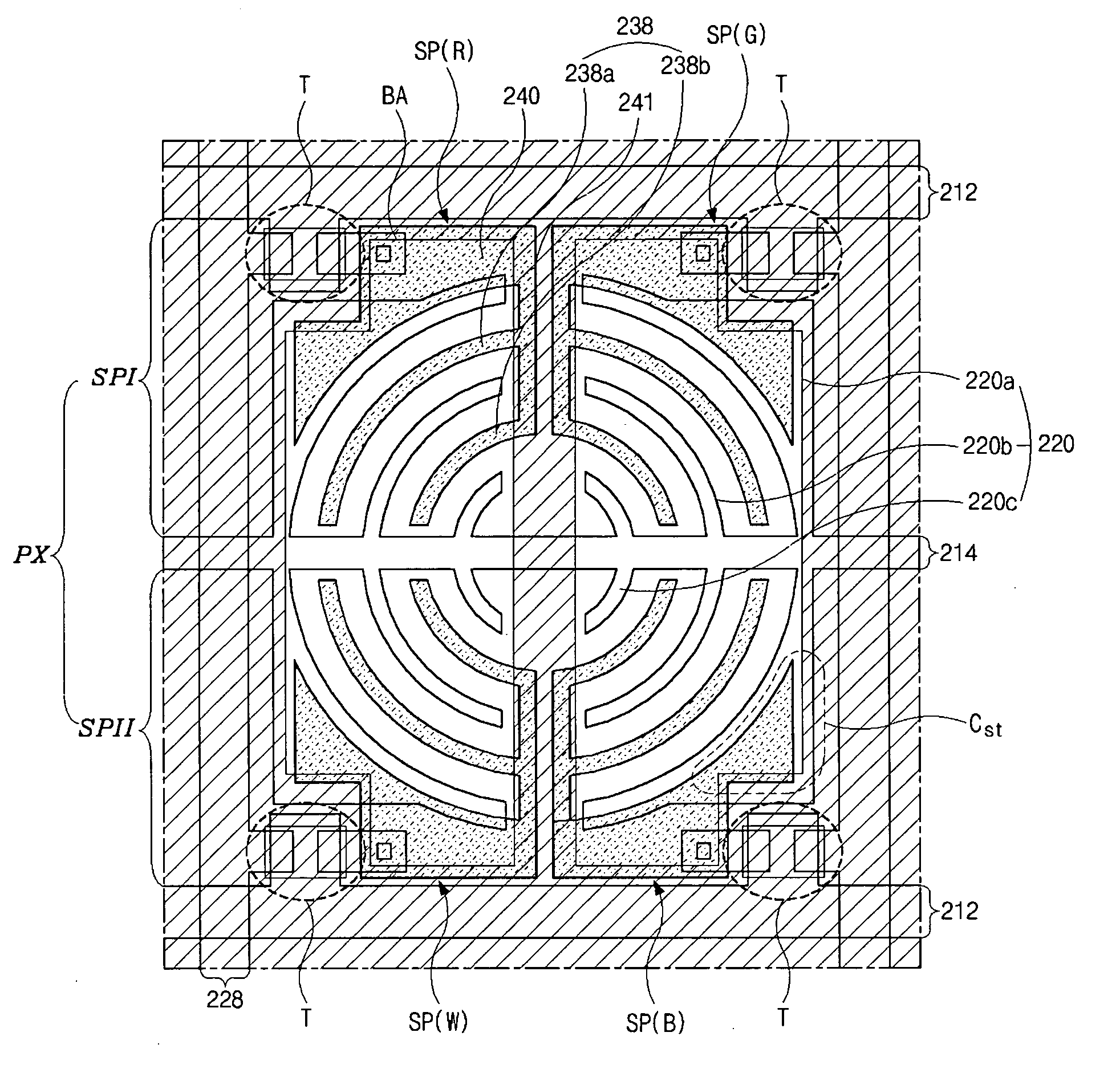
[0049]FIG. 6 is a plan view illustrating one pixel of an array substrate for use in an IPS-LCD device according a second embodiment of the presen...

Example

[0069] In the second embodiment of the present invention, the areas defined between the pixel and common electrodes 338 and 320 are substantially circular shaped in which the liquid crystal directors are uniform in all directions. Thus, color shift is prevented, and the viewing angle is improved in the multiple domains.

[0070] Although the fabrication process illustrated with reference to FIGS. 8A-8E shows a five-mask process, the DD-GG type array substrate for use in the IPS-LCD device may be fabricated using a four-mask process including a diffraction exposure method.

[0071] In accordance with the present invention, color shift is prevented because of the circular areas formed between the arc shaped pixel and common electrodes. Further, because the liquid crystal directors have uniform directions on all sides, the viewing angle is improved and the grain inversion decreases. According to a second embodiment, the aperture ratio of the IPS-LCD device is increased and display images c...


PUM


Abstract

An array substrate for use in an in-plane switching liquid crystal display device includes a plurality of gate lines having a first direction on a substrate; a plurality of data lines having a second direction substantially perpendicular to the plurality of gate lines, wherein pairs of the gate and data lines define a pixel region; a common line in the first direction between the plurality of gate lines; a plurality of common electrodes extending from the common line in the pixel region, wherein the common electrodes have an arc shape; thin film transistors disposed at four corners of the pixel region near crossings of the gate and data lines; a capacitor electrode above a portion of the common electrodes, wherein the capacitor electrode is connected to a corresponding thin film transistor; and a plurality of pixel electrodes connected to the capacitor electrode and disposed between the arc shape of the common electrodes, wherein the pixel electrodes are arc shaped, wherein the pixel region is divided into a plurality of sub pixels, each of which includes one thin film transistor, at least one capacitor electrode, and at least one pixel electrode.

Description

[0001] This application claims the benefit of Korean Patent Application No. 2003-0090359, filed on Dec. 11, 2003, which is hereby incorporated by reference as if fully set forth herein. BACKGROUND OF THE INVENTION [0002] 1. Field of the Invention [0003] The present invention relates to liquid crystal display devices. More particularly, the present invention relates to liquid crystal display devices implementing in-plane switching (IPS) where an electric field applied to liquid crystals is generated in a plane parallel to a substrate. [0004] 2. Discussion of the Related Art [0005] A liquid crystal display device uses the optical anisotropy and polarization properties of liquid crystal molecules to produce an image. Liquid crystal molecules have a definite orientational alignment as a result of their long, thin shapes. The alignment direction can be controlled by an applied electric field. In other words, as an applied electric field changes, so does the alignment of the liquid crysta...

Claims


Application Information

Patent Timeline
IPC IPC(8): G02F1/1343G02F1/1335G02F1/1362G02F1/1368
CPCG02F1/134363G02F2201/52G02F1/136213G02F1/1343
Inventor LEE, YUN-BOKKIM, JEONG-HYUN
Owner LG DISPLAY CO LTD
Why Eureka
Try Eureka