Eureka AIR delivers breakthrough ideas for toughest innovation challenges, trusted by R&D personnel around the world.

System and method for testing electronic devices on a microchip

Inactive Publication Date: 2005-06-23
GOOGLE LLC
View PDF9 Cites 23 Cited by
  • Summary
  • Abstract
  • Description
  • Claims
  • Application Information

AI Technical Summary

Problems solved by technology

The comparison of the plurality of MISR signatures with a plurality of “pass” signatures can take relatively large amounts of computational effort, time, and additional comparison circuitry components.

Method used


Image

  • System and method for testing electronic devices on a microchip
  • System and method for testing electronic devices on a microchip
  • System and method for testing electronic devices on a microchip

Examples


Embodiment Construction

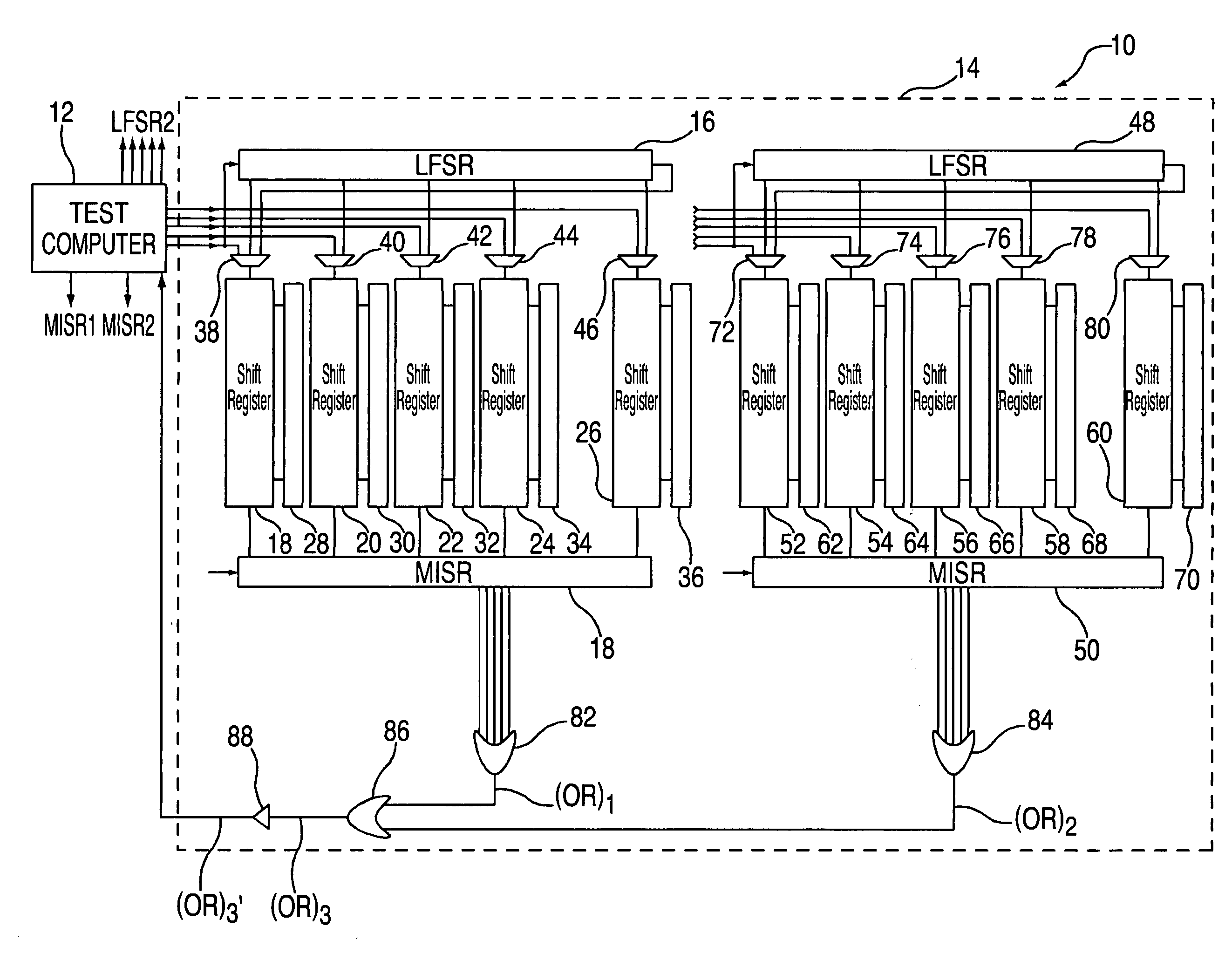
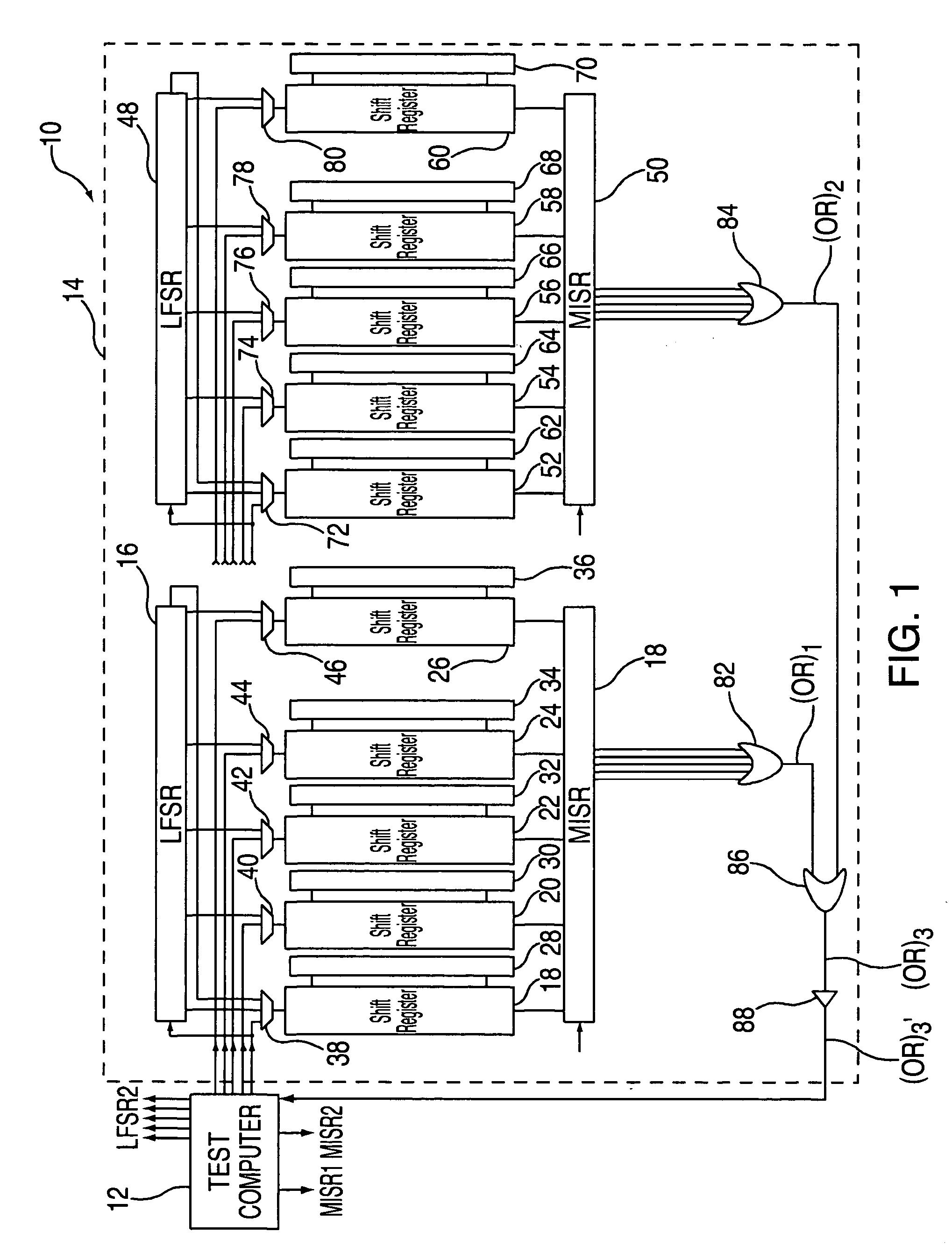
[0014] Referring to the drawings, identical reference numerals represent identical components in the various views. Referring to FIG. 1, a system 10 for testing a microchip includes a test computer 12 and a microchip 14 that utilizes an LBIST test methodology.

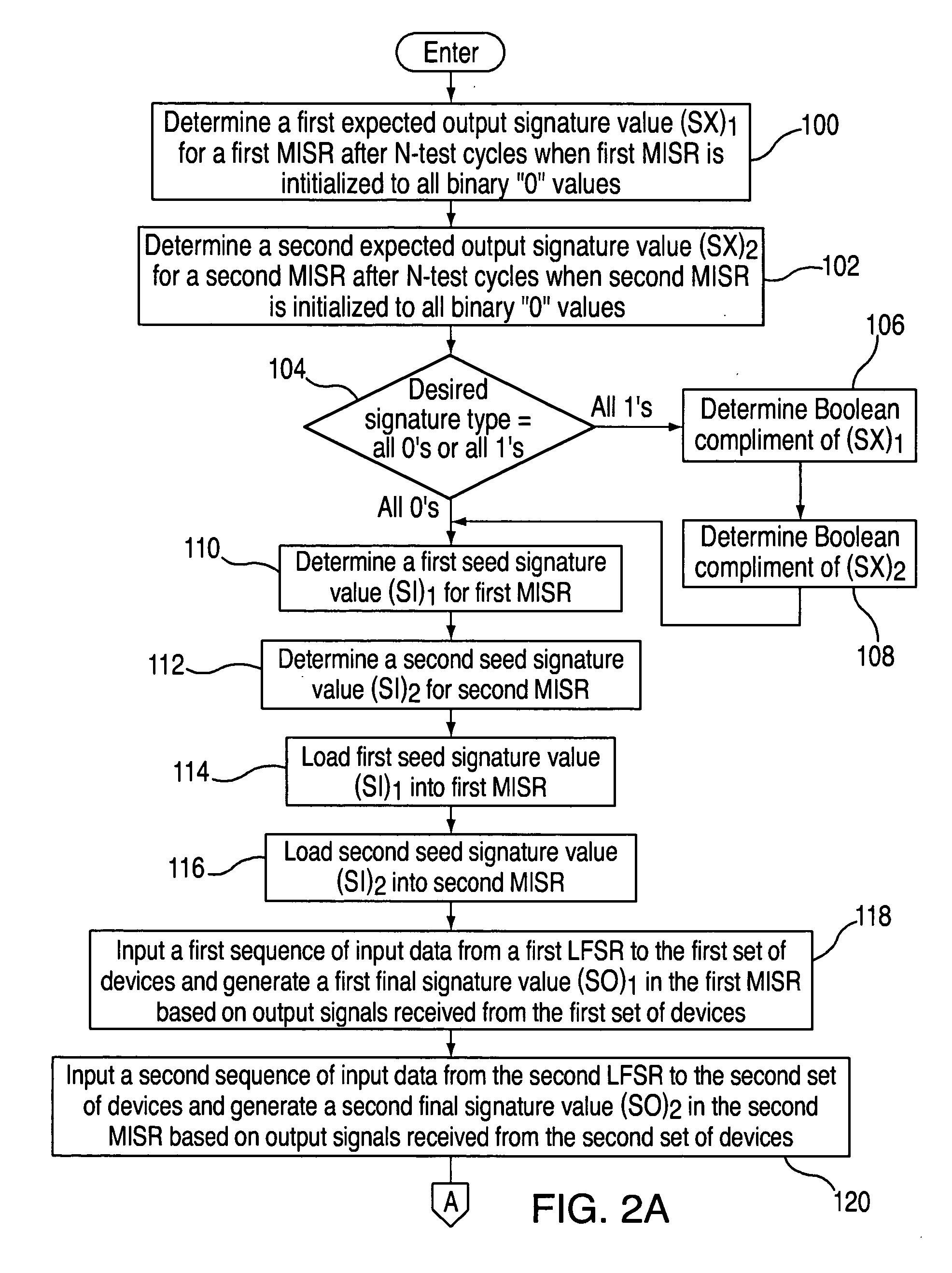
[0015] The test computer 12 is configured to determine first and second initial seed signature values (SX)1, (SX)2 for MISR 18 and MISR 50, respectively, as will be explained in greater detail below.

[0016] Microchip 14 includes LFSR 16, MISR 18, multiplexers 38, 40, 42, 44, 46, latches 17, 20, 22, 24, 26, and first set of devices 28, 30, 32, 34, 36. Microchip 14 further includes LFSR 48, multiplexers 72, 74, 76, 78, 80, shift registers 52, 54, 56, 58, 60, and sets of devices 62, 64, 66, 68, 70. Microchip 14 further includes OR logic gates 82, 84, 86 and buffer driver 88. It should be noted that one or more logic devices may be in both the first set of devices 28, 30, 32, 34, 36 and the second set of devices 62, 64, 66, 68, 70...


PUM


Abstract

A system and method for testing first and second sets of electronic devices on a microchip is provided. The first set of devices receive input data and then send output data to a first multiple input shift register (MISR). The second set of devices receiving input data and then sending output data to a second MISR. The method includes determining a first seed signature value associated with the first MISR that induces the first MISR to have a first final signature value comprising a plurality of identical binary values when the first set of devices send valid output data to the first MISR when receiving a first predetermined sequence of input data. The method further includes determining a second seed signature value associated with the second MISR that induces the second MISR to have a second final signature value comprising a plurality of identical binary values when the second set of devices send valid output data to the second MISR when receiving a second predetermined sequence of input data. The method further includes initializing first and second states of the first MISR and the second MISR, respectively, to the first and second signature values, respectively. The method further includes inputting the first and second predetermined sequences of input data to the first and second set of devices, respectively, and generating first and second final signatures values from output data received from the first and second set of devices, respectively. Finally, the method includes indicating that the first and second set of devices have failed testing when at least one of the plurality of binary values in the first and second final signature values are not identical.

Description

FIELD OF INVENTION [0001] The invention relates to a system and a method for testing electronic devices on a microchip. BACKGROUND OF INVENTION [0002] The development of relatively complex microchips has caused microchip designer's to implement test functionality and test devices within the microchips themselves. The built-in-self-test functions are based on several design-for-test (DFT) techniques such as a (i) logic built-in self-test (LBIST) method for testing combinatorial and sequential logic devices, and (ii) array built-in-self- test (ABIST) for testing memory arrays. [0003] Generally, during the built-in self-testing (BIST) of a microchip, a linear feedback shift register (LFSR) on the chip generates a sequence of pseudo-random binary test data which will be used to stimulate the combinatorial or sequential logic devices or memory arrays in the microchip. The test data is clocked into the combinatorial or sequential logic devices, or memory arrays and the output data receive...

Claims


Application Information

Patent Timeline
IPC IPC(8): G01R31/28G01R31/317G01R31/3185G11C29/40
CPCG01R31/31703G11C29/40G01R31/318566
Inventor MOTIKA, FRANCOHUOTT, WILLIAM VINCENT
Owner GOOGLE LLC
Why Eureka
Eureka Blog
Learn More