Logic circuit utilizing pass transistors and logic gate

Inactive Publication Date: 2000-07-04
KAWASAKI MICROELECTRONICS
View PDF19 Cites 217 Cited by
  • Summary
  • Abstract
  • Description
  • Claims
  • Application Information

AI Technical Summary

Problems solved by technology

This poses the problem that it becomes hard to verify the operating timing of a logic circuit.
However, intense restrictions are imposed on such product terms containing a large number of variables.
It is hard to efficiently express various logical operations with them.
In addition, power consumption by the logic circuit in the succeeding stage creases, and a noise margin decreases.
Furthermore, it is a problem that the logical amplitude (difference in potential between HIGH and LOW states) of an output logic signal decreases.
However, when the pull-up or pull-down is thus carried out, the problem arises that load capacitance relative to a logic circuit in a preceding stage becomes larger, signal delay is extended, and power consumption and chip area increase.
The inventor has recognized a problem that the number of required switching devices in conventional pass-transistor logic circuits can become larger

Method used


Image

  • Logic circuit utilizing pass transistors and logic gate
  • Logic circuit utilizing pass transistors and logic gate
  • Logic circuit utilizing pass transistors and logic gate

Examples


first embodiment

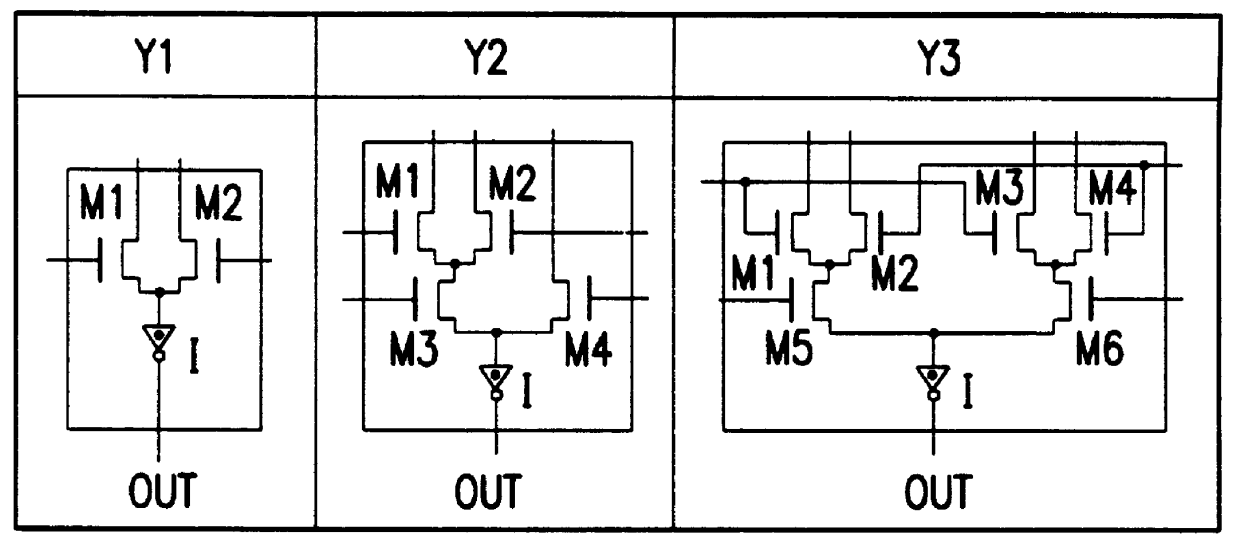
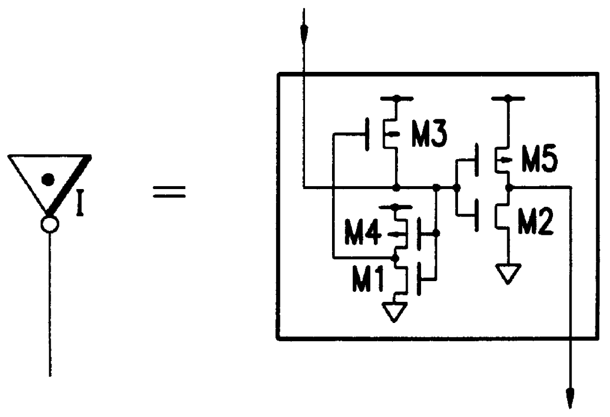
FIG. 12 is a circuit diagram of a logic circuit of the present invention. This logic circuit includes two single-stage pass-transistor logic trees. N-channel MOS transistors and P-channel MOS transistors employed are enhancement mode MOS transistors whose threshold voltages are on a level with those of MOS transistors employed in a conventional CMOS logic circuit. For example, when a supply voltage (=power supply potential-reference potential) is 3.3 V, the threshold voltages of the N-channel MOS transistors and P-channel MOS transistors are typically 0.55 V and -0.55 V, respectively.

N-channel MOS transistors M1 and M2 constitute a first pass-transistor logic tree. In the first pass-transistor logic tree, the sources and gates of the transistors M1 and M2 act as input nodes and receive logic signals a, b, c, and c. The drains of the transistors M1 and M2 are coupled, thus forming an intermediate output node. The logic signals a and b can be mutually independent, while the logic sign...

second embodiment

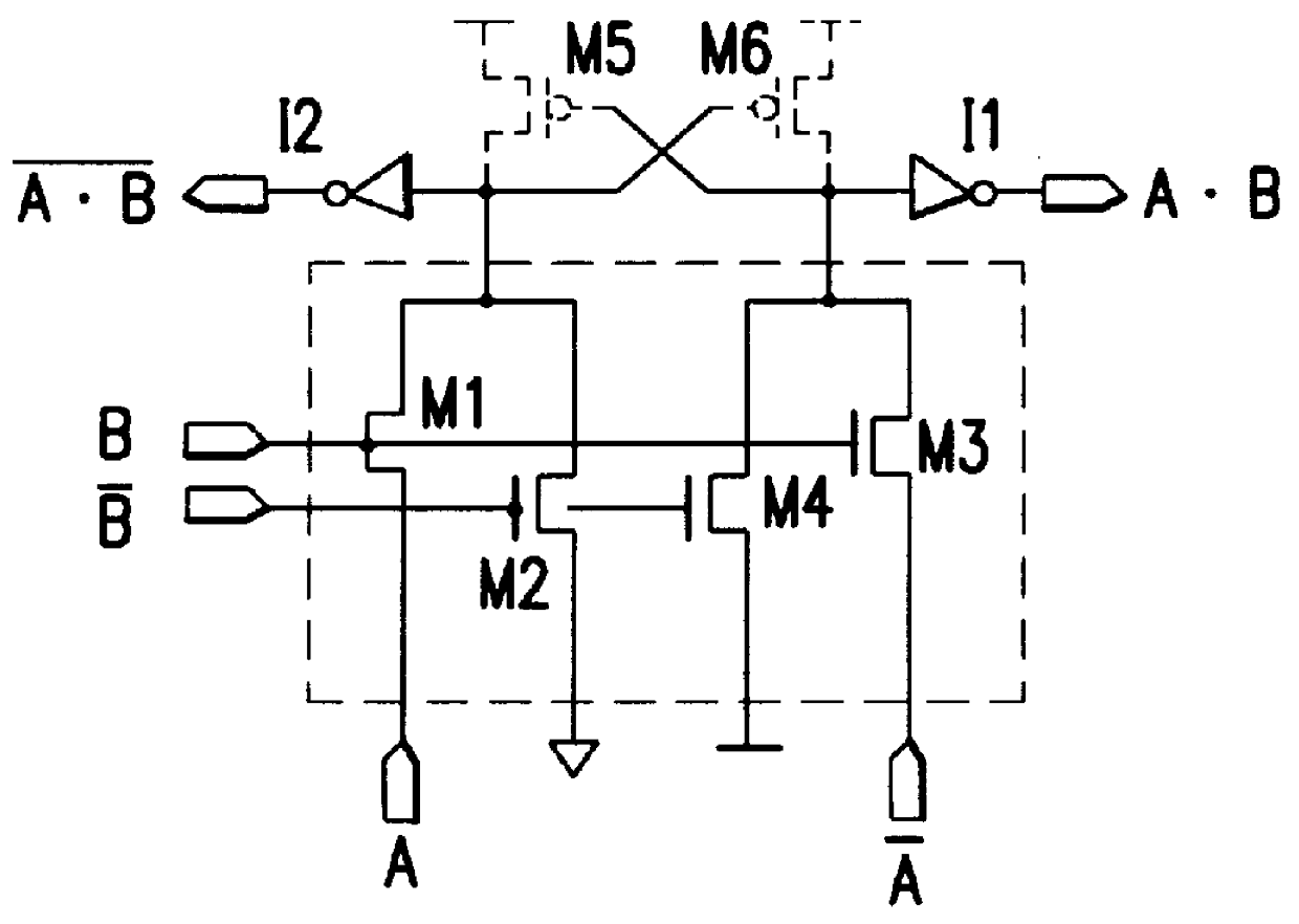
FIG. 16 is a circuit diagram of a logic circuit of the present invention having two single-stage pass-transistor logic trees.

Each of T1 and T2 in the drawing denotes a circuit (hereinafter, a pair pass transistor element) enclosed in a square drawn with a dot-dash line in FIG. 17. Here, an N-channel MOS transistor M1A and P-channel MOS transistor M1B are connected in parallel with their sources and drains coupled, thus forming a first unit pass transistor. An N-channel MOS transistor M2 A and P-channel MOS transistor M2B are connected in parallel with their sources and drains coupled, thus forming a second unit pass transistor. The output terminals (drains) of the first and second unit pass transistors are coupled. A pair pass transistor element T is thus configured. The N-channel MOS transistor and P-channel MOS transistor constituting each unit pass transistor are connected so that they can receive two input signals P and Q, which are mutually complementary, through the gates ther...


PUM


Abstract

A logic circuit combines a plurality of pass-transistor logic trees and a multiple-input logic gate for receiving intermediate logic signals from the respective pass-transistor logic trees, and can express a complex logical operation while decreasing the number of stages in pass-transistor logic trees and improving operation speed. Even a logical operation that cannot be expressed efficiently by a known or conventional pass-transistor logic circuit can be expressed efficiently with performance higher than that of a known CMOS logic circuit. Furthermore, when a static feedthrough current of the multiple-input logic gate is suppressed, power consumption can be reduced. In some embodiments, since circuitry for suppressing a static feedthrough current of the multiple-input logic gate is arranged so that a probability of occurrence of logical collision with a preceding stage will decrease or will be nil, power consumption can further be reduced.

Description

1. Field of the InventionThe present invention relates to a logic circuit using switching devices, in each of which conduction between an input terminal and output terminal is turned ON or OFF according to a potential at a control terminal, as pass transistors to realize desired logic. In particular, this invention is concerned with a logic circuit capable of realizing complex logic while improving operation speed by decreasing the number of stages of pass transistors required to be connected in series. Furthermore, the present invention relates to a logic circuit capable of realizing logic functions, for which many transistors are needed in conventional pass-transistor logic circuits, using a smaller number of transistors, and having characteristics of high operation speed and small power consumption.2. Description of the Related ArtWhat is referred to as a "pass-transistor logic circuit" that aims to minimize the number of circuit elements or improve operation speed has been sugge...

Claims


Application Information

Patent Timeline
IPC IPC(8): H03K19/094H03K19/20H01L21/8238H01L27/092H03K19/0952H03K19/173
CPCH03K19/1737
Inventor SAKO, NORIMITSU
Owner KAWASAKI MICROELECTRONICS
Why Eureka
Try Eureka