Complementary logic gate device

a logic gate and gate device technology, applied in the direction of semiconductor devices, electrical devices, nanotechnology, etc., can solve the problems of inability to realize a logic operation equivalent to cmos, inability to achieve a logic operation equivalent to graphene, and inability to realize an n-type or p-type semiconductor characteristic having sufficient carrier concentration, etc., to achieve the effect of low power consumption

Inactive Publication Date: 2012-07-24
OTSUJI TAIICHI +1
View PDF10 Cites 5 Cited by
  • Summary
  • Abstract
  • Description
  • Claims
  • Application Information

AI Technical Summary

Benefits of technology

[0021]In the present invention, without using an n-type or a p-type semiconductor, thus, without using a p-type channel FET or an n-type channel FET, graphene is introduced into an electron channel layer of the FET (hereinafter referred to as a graphene channel FET), and by utilizing an ambipolar characteristic (single pole bilateral characteristic operating in an electron mode and a hole mode) of a graphene material so as to replace a p-type channel FET and an n-type channel FET in the prior-art CMOS logic gate by two graphene channel FETs with different threshold values, a complementary logic operation equivalent to the CMOS is realized.

Problems solved by technology

However, in recent years when a characteristic dimension of the FET (electric field effect transistor) is approaching 10 nm at which a quantum-mechanical tunnel effect might be incurred, it has already become difficult to achieve speed-up by miniaturization of an element.
However, graphene cannot realize a logic operation equivalent to CMOS by substituting MOSFET as it is due to the following two points.
The first point is that since doping of impurities is extremely difficult, it is only a so-called intrinsic semiconductor characteristic that can be provided, and realization of an n-type or p-type semiconductor characteristic having sufficient carrier concentration is extremely difficult (See Non-Patent Documents 1, 4, and 5, for example).
Due to the above reasons, in a FET having a graphene material as an electron channel layer (channel), a configuration of a CMOS logic gate composed of a p-type channel FET and an n-type channel FET is impossible, and thus, a configuration of a CMOS-compatible complementary gate which can realize the current ultra low power consumption and super large integration has been impossible.

Method used


Image

  • Complementary logic gate device
  • Complementary logic gate device
  • Complementary logic gate device

Examples


Embodiment Construction

[0029]A complementary logic gate device of embodiments of the present invention will be described below referring to the attached drawings.

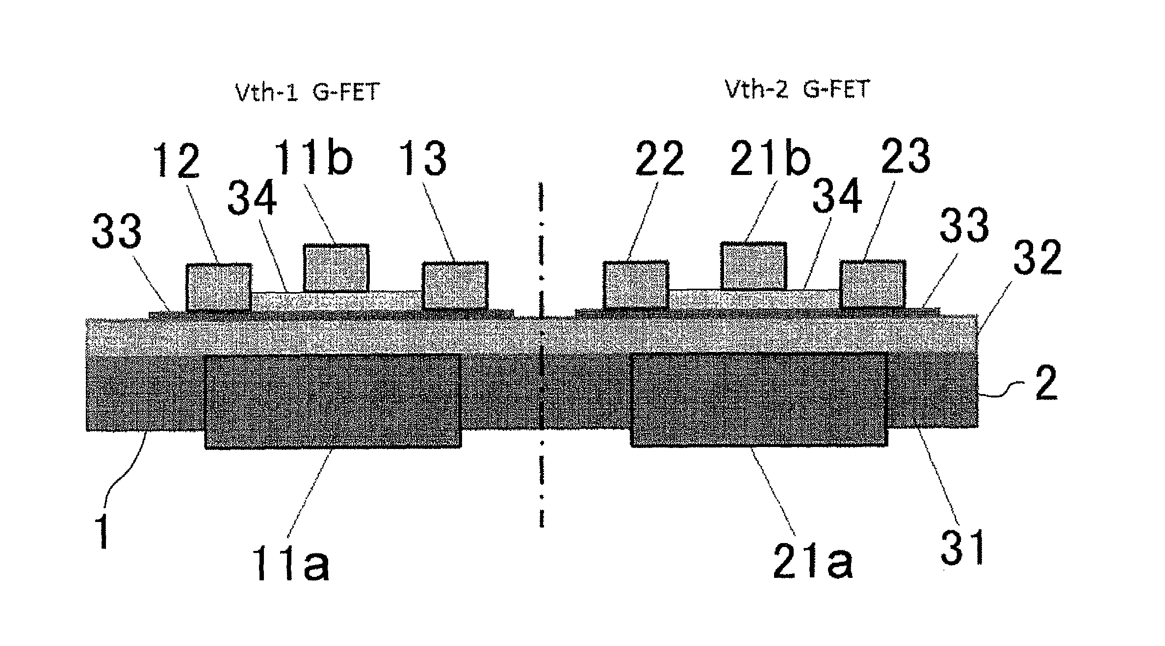
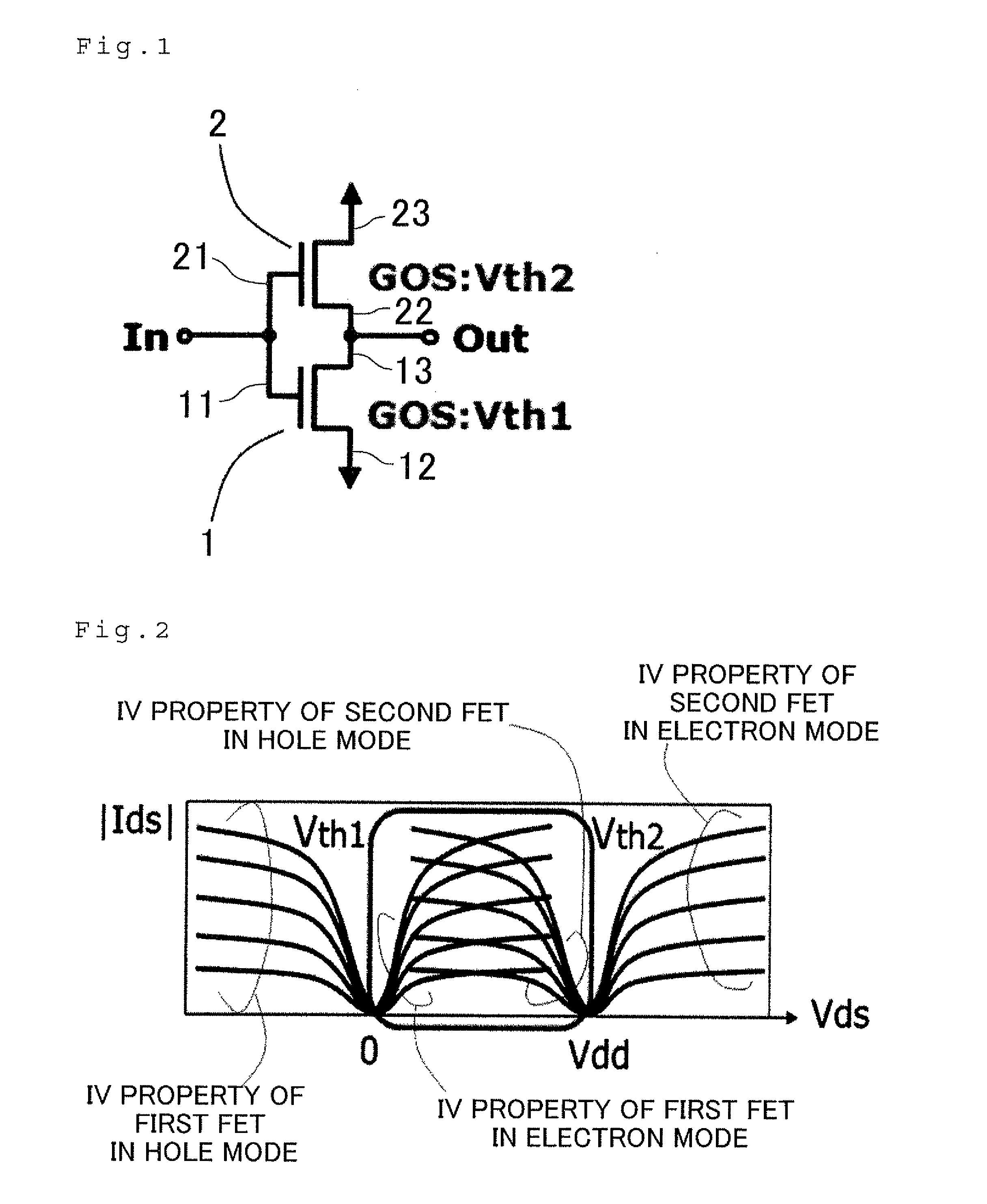
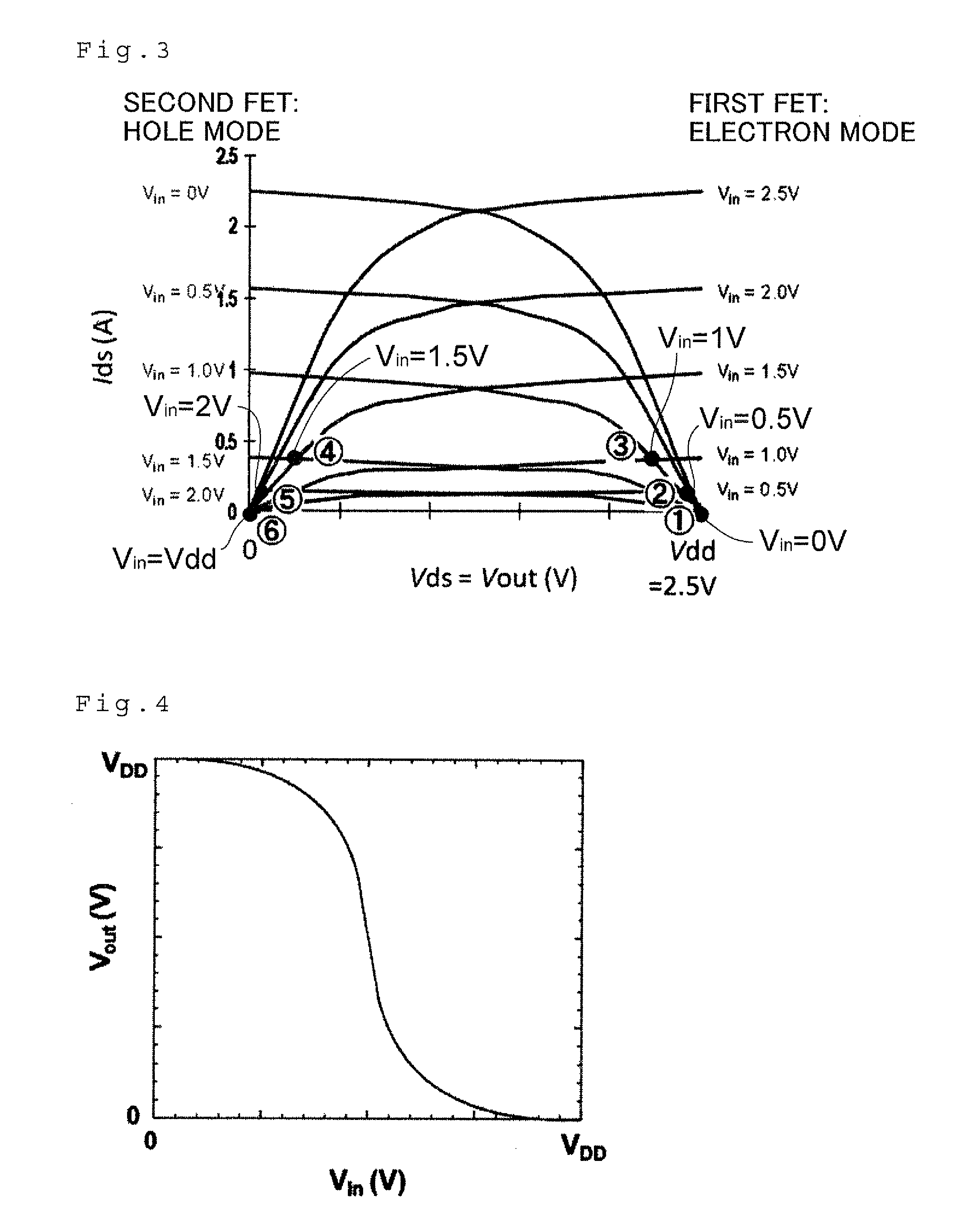
[0030]FIG. 1 shows a configuration example of the complementary logic gate device illustrating a first embodiment of the present invention. For example, two FETs, that is, a first FET 1 and a second FET 2 with an electron channel layer formed by graphene, an ambipolar characteristic (single pole bilateral characteristic), and different threshold values, are prepared. Supposing that threshold voltages of the first FET 1 and the second FET 2 are Vth1 and Vth2, respectively, drain current-drain voltage characteristics of the first FET 1 and the second FET 2 have, as the FET current-voltage characteristic of the complementary logic gate device illustrating the first embodiment of the present invention shown in FIG. 2, a so-called ambipolar (single pole bilateral) characteristic in which an FET characteristic by electron transport of a region: Vds>Vth...


PUM


Abstract

Provided is a complementary logical gate device represented by a silicon CMOS logical circuit among semiconductor integrated logical circuits which can effectively solve the problem of the speed performance limit of an ultra-large scale integration and an ultra-low power consumption type logical circuit. The complementary logical gate includes an electron running layer formed by grapheme without using an n-channel FET or a p-channel FET, has the ambipolar characteristic, and uses only two FET having different threshold values, i.e., a first FET and a second FET. The first FET has a gate electrode short-circuited to a gate electrode of the second FET so as to constitute an input terminal. The first FET has a source electrode set to a low potential. The first FET has a drain electrode connected to a source electrode of the second FET so as to constitute an output terminal. The second FET has a drain electrode set to a high potential.

Description

TECHNICAL FIELD[0001]The present invention relates to a semiconductor integrated logic circuit and particularly to a complementary logic gate device useful in overcoming a speed performance limitation of an ultra large-scale integration and ultra low power consumption integrated logic device composed of a complementary logic gate device represented by a silicon CMOS (complementary metal oxide film Semiconductor) logic circuit.BACKGROUND ART[0002]Since a silicon CMOS logic gate device has both ultra large-scale integration and ultra low power consumption performances, it forms a core of the current semiconductor integrated circuit technology. As in a configuration example of the logic gate device in the prior-art technology shown in FIG. 6, in the CMOS logic gate, by combining and complementarily operating an n-type channel MOSFET (metal oxide film semiconductor type electric field effect transistor) and a p-type channel MOSFET, such a characteristic is provided that an operating cur...

Claims


Application Information

Patent Timeline
Patent Type & Authority Patents(United States)
IPC IPC(8): H01L29/08
CPCH01L21/8213H01L27/1203H01L29/78684H01L27/11807H01L27/092Y10S977/734H01L21/8228
Inventor OTSUJI, TAIICHISANO, EIICHI
Owner OTSUJI TAIICHI
Why Eureka
Try Eureka