Optical device and circuit using phase modulation and related methods

a phase modulation and optical device technology, applied in the field of optical devices, can solve the problems of affecting the stability of logic state representation, affecting the ability to represent logic state stably for as long as may be required, and affecting the performance of logic circuits

Inactive Publication Date: 2005-11-24
COVEY JOHN
View PDF54 Cites 70 Cited by
  • Summary
  • Abstract
  • Description
  • Claims
  • Application Information

AI Technical Summary

Benefits of technology

[0025] An optical NAND gate in accordance with an embodiment of the invention comprises first, second, third, and fourth photonic transistors. The first photonic transistor receives a first optical input signal and an optical reference signal and generating a first optical output signal based thereon. The second optical transistor receives the first optical output signal and the second optical input signal, and generating a second optical output signal based thereon. A first phase shift element shifts the phase of the optical reference signal by π radians relative to the phase of the optical reference signal input to the first transistor. The third transistor generates a third optical output signal based on the phase-shifted optical reference signal and the first optical input signal. A second phase shift element shifts the phase of the optical reference signal by π radians relative to the phase of the optical reference signal input to the first transistor. The fourth transistor generates a fourth optical output signal based on the second optical input signal and the phase-shifted optical reference signal. One of the second, third, and fourth optical output signals is provided to the output pathway as the output of the NAND gate. The first, second, third, and fourth photonic transistors can be defined in a guiding element having spaced structures arranged according to the wavelength of the first and second optical input signals and the optical reference signal propagating in the NAND gate. The spaced structures of the guiding element can optically isolate the first, second, third, and fourth optical transistors from one another. The guiding element can define at least one pathway guiding one of the signals propagating in the optical NAND gate which turns at an angle of at least π / 3 radians. The periodic spacing of the guiding element can filter at least one wavelength other than the wavelength of the first and second optical input signals and the optical reference signal.

Problems solved by technology

However, use of optical devices to form integrated logic circuits presents unique challenges.
The ability to represent a logic state stably for as long as may be required thus becomes an issue.
Although guiding elements are interesting from the standpoint that they automatically filter light of undesired wavelengths, an undesired result is that light is quickly attenuated in guiding elements.
Although conductive electrical wires and the like can turn abruptly in connecting to electrical transistors, optical waveguides can not generally turn so abruptly without use of mirrors because excessive light will escape the waveguide.
Thus, integrated optical waveguides have limits on how abruptly they can turn which further impacts on the size of the integrated device and creates issues regarding optical isolation of the integrated devices.
The problem with such an approach is that it requires very stringent control on the amplitudes of the optical signals on which logic operations are performed.
This approach for an optical modulation scheme is not generally desirable because of the complications associated with maintaining appropriate amplitude levels throughout the circuit.
The Asakawa device represents binary zeros with the lack of light, which cannot be used to perform digital logic, because the device transmits no data if no light enters it.
Although Romaniuk's device is meritorious in several respects, it requires use of both phase and amplitude modulated inputs to perform complex logic operations, and thus requires a linear absorber to discern logic levels.
More specifically, in the Romaniuk device, if two signals interfere constructively, the magnitude of the output becomes twice as large.
If this interference continues to propagate through a circuit as it does in the Romaniuk device, complications result when it is used as an input to a subsequent logic gate with an amplitude twice as large as it was originally.
However, this requires exacting control of the amplitude of the logic levels in the device through the use of a linear optical absorber.

Method used


Image

  • Optical device and circuit using phase modulation and related methods
  • Optical device and circuit using phase modulation and related methods
  • Optical device and circuit using phase modulation and related methods

Examples


Embodiment Construction

[0039] The present inventions now will be described more fully hereinafter with reference to the accompanying drawings, in which some, but not all embodiments of the invention are shown. Indeed, these inventions may be embodied in many different forms and should not be construed as limited to the embodiments set forth herein; rather, these embodiments are provided so that this disclosure will satisfy applicable legal requirements. Like numbers refer to like elements throughout.

Definitions

[0040]‘And / or’ means ‘one, some, or all’ of the things immediately preceding and succeeding this phrase. Thus, ‘A, B and / or C’ means ‘any one, some or all of A, B, and C.’

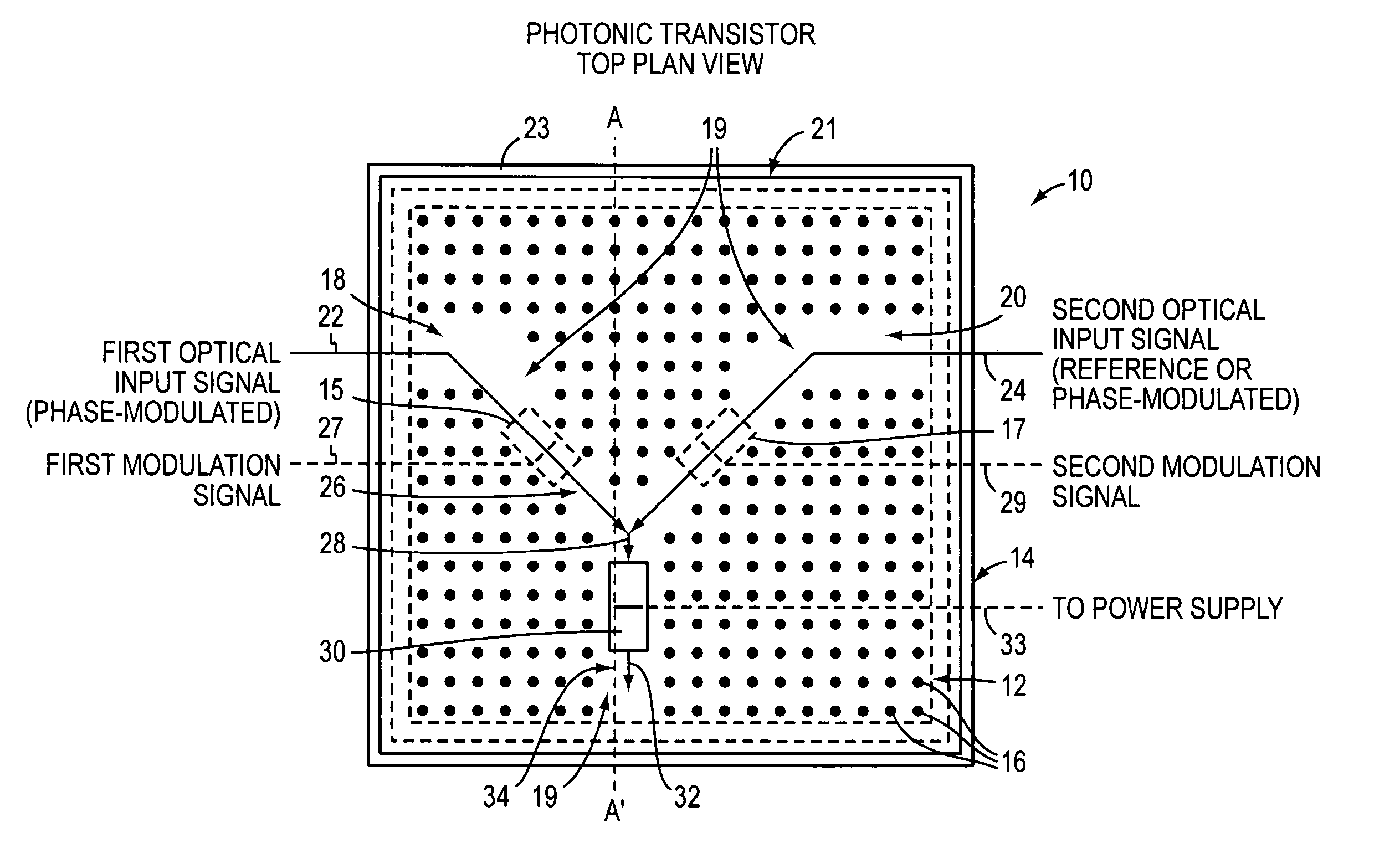
[0041]‘Downstream’ refers to a position or element that is further along an optical transmission path relative to a reference point. It can also used to refer to the direction of travel of light in an optical device away from a reference point.

[0042]‘Substrate’ is a workpiece or starting material upon which a photonic bandgap (P...


PUM

PropertyMeasurementUnit
phaseaaaaaaaaaa
optical interferenceaaaaaaaaaa
phase modulationaaaaaaaaaa

Abstract

A disclosed apparatus comprises a guiding element and a nonlinear element. The guiding element guides optical input signals, at least one of which is phase-modulated, to an interference area where such signals meet and interfere. The resulting interference signal is nonlinearly discriminated by the nonlinear element to produce an optical output signal that can be amplitude- or phase-modulated according to the phase modulation of the input signals. The invention also includes related methods and photonic logic gates.

Description

BACKGROUND OF THE INVENTION [0001] 1. Field of the Invention [0002] This invention relates to an optical device functioning as a photonic transistor. The invented optical device can be used as a basic element in an optical integrated circuit (OIC) that permits logic operations to be carried out using optical signals. [0003] 2. Description of the Related Art [0004] In electronic devices, transistors are the basic elements of circuits. In digital applications, a transistor has the properties of a switch. The transistor can be driven between conductance and non-conductance states in order to change the voltage level, and thereby logic level, output by the transistor. [0005] Interest has begun to emerge in recent years toward development of an optical device that behaves analogously to a electronic transistor. The reason for this interest is that optical signals can potentially travel faster in integrated circuits than electrical signals because they are not subject to capacitance which...

Claims


Application Information

Patent Timeline
Patent Type & Authority Applications(United States)
IPC IPC(8): G02F3/00G02F3/02H04B10/04
CPCG02F3/00G02F2202/32G02F3/024
Inventor COVEY, JOHN LUTHER
Owner COVEY JOHN
Why Eureka
Try Eureka