Semiconductor device, power diode, and rectifier

a technology of power diodes and semiconductor devices, applied in the field of semiconductor devices, can solve the problems of difficult to obtain crystals with good quality, high process temperature for manufacturing semiconductor devices, and inability to form insulating layers with good quality by thermal oxidation, etc., to achieve higher on-state current, lower reverse saturation current, and high withstand voltage

Active Publication Date: 2012-03-15
SEMICON ENERGY LAB CO LTD
View PDF1 Cites 38 Cited by
  • Summary
  • Abstract
  • Description
  • Claims
  • Application Information

AI Technical Summary

Benefits of technology

[0028]A semiconductor which has characteristics such as higher withstand voltage and lower reverse saturation current and can have higher on-state current as compared to a conventional semiconductor device can be provided. In addition, a semiconductor device in which degradation due to heat generation can be suppressed can be provided.

Problems solved by technology

A semiconductor device for high power application needs various electrical characteristics such as high withstand voltage, low reverse saturation current, and high on-state current, but so many problems arise when a semiconductor device having such electrical characteristics is actually manufactured.
For example, silicon carbide has problems in that it is difficult to obtain a crystal with good quality and a process temperature for manufacturing a semiconductor device is high.
In addition, since carbon is contained, there is a problem in that an insulating layer with good quality cannot be formed by thermal oxidation.
Furthermore, silicon carbide is chemically very stable and is not easily etched by normal wet etching.

Method used


Image

  • Semiconductor device, power diode, and rectifier
  • Semiconductor device, power diode, and rectifier
  • Semiconductor device, power diode, and rectifier

Examples


embodiment 1

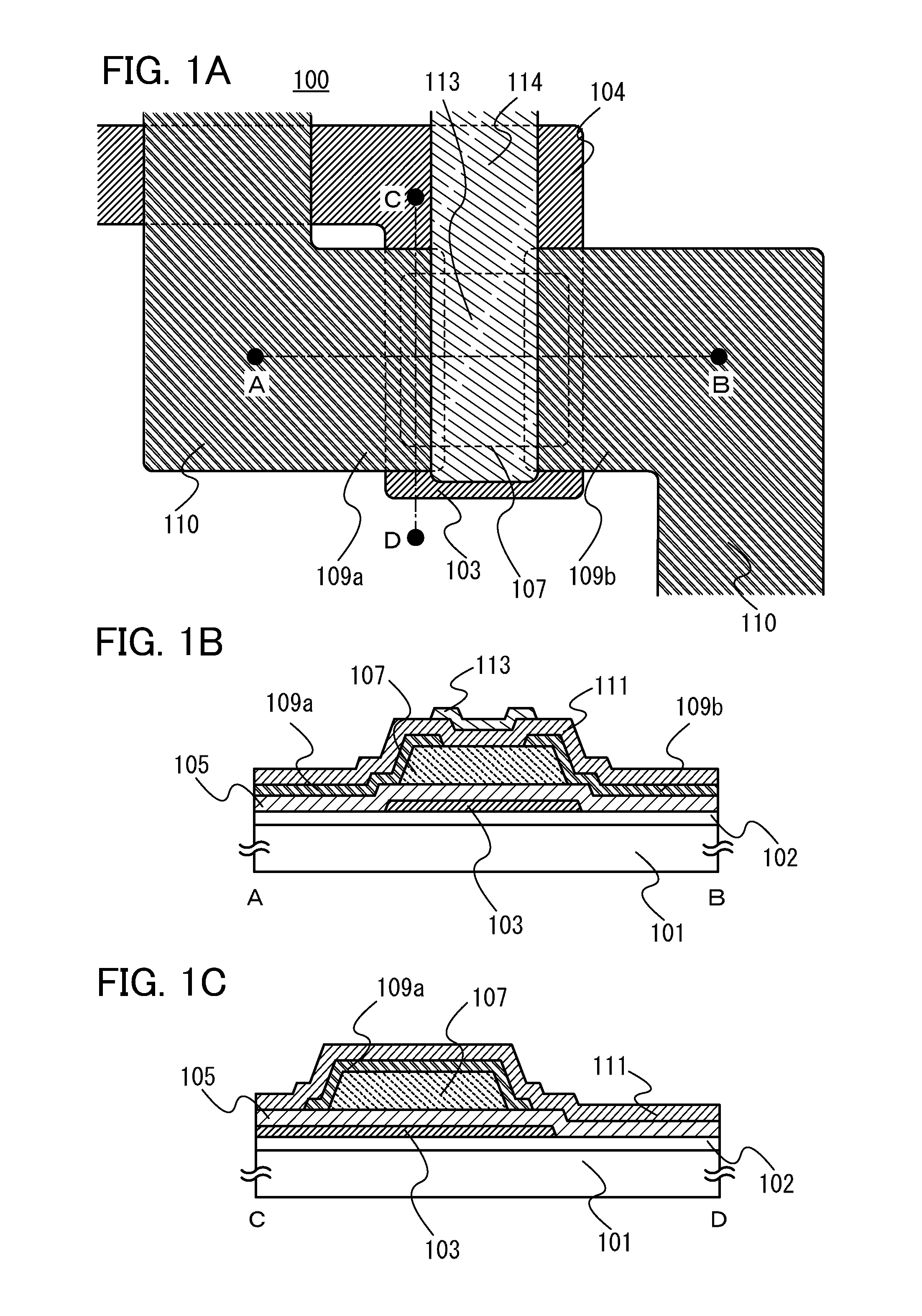
[0055]In this embodiment, a structure of a non-linear element that is one embodiment of the present invention and a method for manufacturing the non-linear element will be described with reference to FIGS. 1A to 1C, FIGS. 2A to 2D, and FIGS. 3A to 3D. Note that a transistor is described as an example in this embodiment.

[0056]FIG. 1A is a plan view of a transistor 100, and FIG. 1B is a cross-sectional view taken along line A-B in the transistor 100. FIG. 1C is a cross-sectional view taken along line C-D in the transistor 100. Note that a base insulating layer 102, a gate insulating layer 105, and an insulating layer 111 are not illustrated in FIG. 1A for convenience. FIG. 1A illustrates a wiring 104 including a first electrode 103 functioning as a gate electrode; an oxide semiconductor layer 107 including a channel formation region; a wiring 110 including a pair of second electrodes 109a and 109b functioning as a source electrode and a drain electrode; and a wiring 114 provided betwe...

embodiment 2

[0141]In this embodiment, a non-linear element whose structure is partly different from that of the non-linear element described in Embodiment 1 will be described. Note that a transistor is used as an example also in this embodiment.

[0142]FIG. 4A is a plan view of a transistor 200, and FIG. 4B is a cross-sectional view taken along line E-F in the transistor 200. FIG. 4C is a cross-sectional view taken along line G-H in the transistor 200. Note that the transistor 200 is a modified example of the transistor 100; therefore, in FIGS. 4A to 4C, the same reference numerals are used for the same parts as those in FIGS. 1A to 1C, and detailed description of the same reference numerals is omitted.

[0143]As illustrated in FIG. 4B, the transistor 200 is a dual-gate transistor and includes a base insulating layer 102, a first electrode 103, a gate insulating layer 105, an oxide semiconductor layer 107, n+ layers 117a and 117b, a pair of second electrodes 109a and 109b, an insulating layer 111, ...

embodiment 3

[0154]In this embodiment, a non-linear element whose structure is partly different from that of the non-linear element described in Embodiment 1 will be described. Note that a transistor is used as an example also in this embodiment.

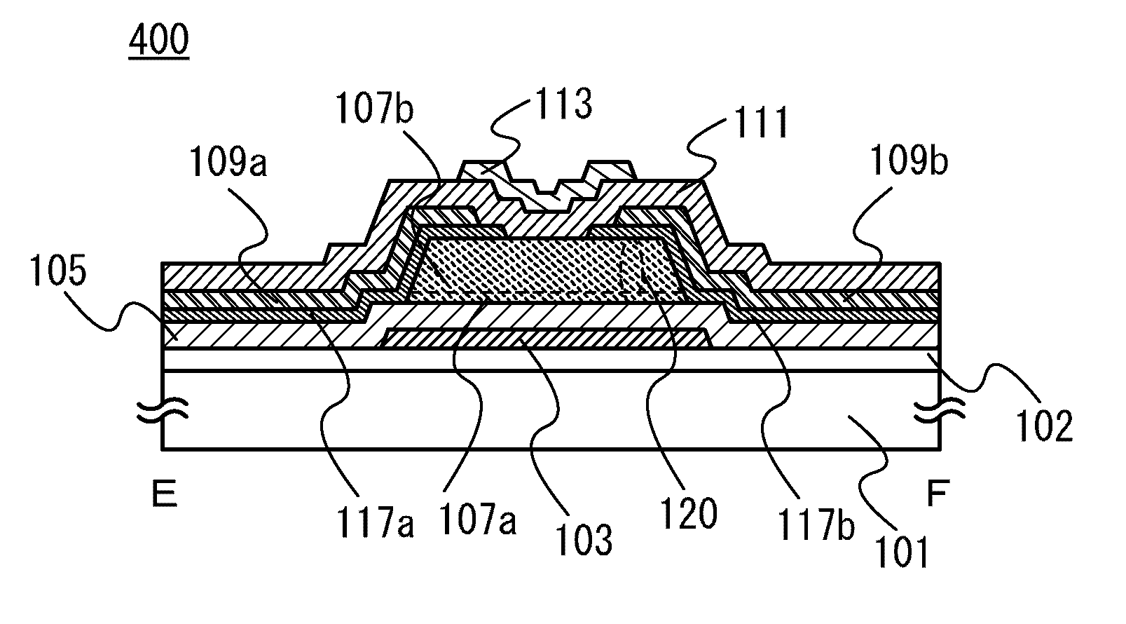
[0155]A transistor 300 described in this embodiment is a transistor obtained in such a manner that the oxide semiconductor layer 107 of the transistor 100 described in Embodiment 1 is replaced with a crystalline oxide semiconductor stack 120 including a first crystalline oxide semiconductor layer 107a and a second crystalline oxide semiconductor layer 107b. In short, a plan structure of the transistor 300 is similar to that of the transistor 100; therefore, FIG. 1A can be referred to for the plan view of the transistor 300. FIG. 6A is a cross-sectional view taken along line A-B in the transistor 300. FIG. 6B is a cross-sectional view taken along line C-D in the transistor 300. Note that the transistor 300 is a modified example of the transistor 100; ther...


PUM


Abstract

An object is to provide a semiconductor device having electrical characteristics such as high withstand voltage, low reverse saturation current, and high on-state current. In particular, an object is to provide a power diode and a rectifier which include non-linear elements. An embodiment of the present invention is a semiconductor device including a first electrode, a gate insulating layer covering the first electrode, an oxide semiconductor layer in contact with the gate insulating layer and overlapping with the first electrode, a pair of second electrodes covering end portions of the oxide semiconductor layer, an insulating layer covering the pair of second electrodes and the oxide semiconductor layer, and a third electrode in contact with the insulating layer and between the pair of second electrodes. The pair of second electrodes are in contact with end surfaces of the oxide semiconductor layer.

Description

BACKGROUND OF THE INVENTION[0001]1. Field of the Invention[0002]The technical field of the present invention relates to a semiconductor device using an oxide semiconductor.[0003]In this specification, the semiconductor device refers to all the devices that operate by utilizing semiconductor characteristics. In this specification, a transistor is included in a non-linear element, the non-linear element is a semiconductor device, and an electrooptic device, a semiconductor circuit, and an electronic appliance including the non-linear element are all included in semiconductor devices.[0004]2. Description of the Related Art[0005]Many of transistors included in display devices typified by flat panel displays (e.g., liquid crystal display devices and light-emitting display devices) include silicon semiconductors such as amorphous silicon or polycrystalline silicon and are formed over glass substrates.[0006]Attention has been directed to a technique by which, instead of such silicon semico...

Claims


Application Information

Patent Timeline
Patent Type & Authority Applications(United States)
IPC IPC(8): H01L29/78
CPCH01L29/24H01L29/7869H01L29/78648H01L29/42356
Inventor YAMAZAKI, SHUNPEIGODO, HIROMICHIKOBAYASHI, SATOSHI
Owner SEMICON ENERGY LAB CO LTD
Why Eureka
Try Eureka