Dual mode analog differential and CMOS logic circuit

a logic circuit and analog differential technology, applied in logic circuit coupling/interface arrangement, instruments, pulse techniques, etc., can solve the problems of insufficient testing of the first functional analog differential circuit, difficulty or impossible and inability to apply to analog differential circuitry

Active Publication Date: 2005-05-26
INTELLECTUAL DISCOVERY INC
View PDF2 Cites 4 Cited by
  • Summary
  • Abstract
  • Description
  • Claims
  • Application Information

AI Technical Summary

Benefits of technology

[0005] A principal object of the present invention is to provide a dual mode, analog differential and complementary metal oxide semiconductor (CMOS) logic circuit. Other important objects of the present invention are to provide such dual mode, analog differential and complementary metal oxide semiconductor (CMOS) logic circuit substantially without negative effect and that overcome many of the disadvantages of prior art arrangements.

Problems solved by technology

These testing rules are intended for complementary metal oxide semiconductor (CMOS) logic circuits and generally are difficult or impossible to apply to analog differential circuitry.
Significant disadvantages of this approach are that the first functional analog differential circuit is not really tested, and extra circuitry is required for the CMOS duplicate circuit and the selection switch.
Also the capacitive loads of the selection circuitry compromise the performance of the functional analog differential circuit.

Method used


Image

  • Dual mode analog differential and CMOS logic circuit
  • Dual mode analog differential and CMOS logic circuit
  • Dual mode analog differential and CMOS logic circuit

Examples


Embodiment Construction

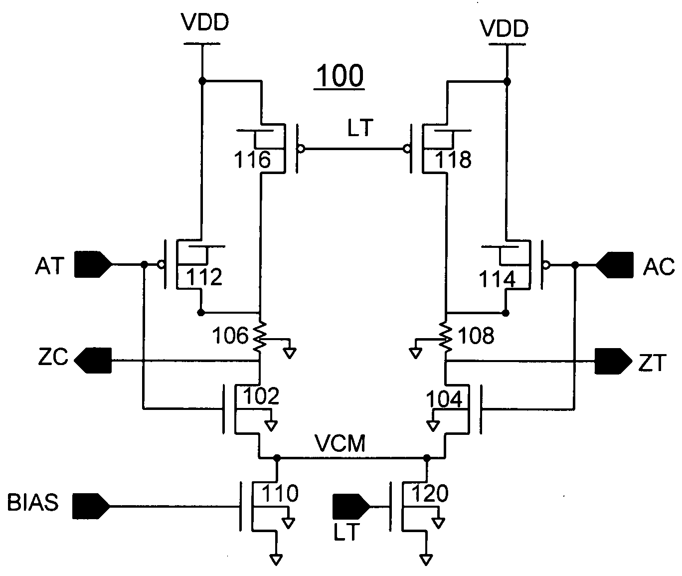
[0010] Having reference now to the drawings, in FIG. 1 there is shown an exemplary dual mode, analog differential and complementary metal oxide semiconductor (CMOS) logic circuit in accordance with the preferred embodiment generally designated by the reference character 100. Dual mode, analog differential and CMOS logic circuit 100 functions normally as an analog differential circuit and functions as CMOS logic for test purposes.

[0011] In accordance with features of the preferred embodiment, dual mode, analog differential and CMOS logic circuit 100 continues to function during leak testing where no DC current is allowed. Typically analog differential circuits require DC current and therefore are not functional during leak testing. Dual mode, analog differential and CMOS logic circuit 100 allows a no DC current mode or CMOS mode for test purposes. Dual mode, analog differential and CMOS logic circuit 100 functions as an analog differential circuit providing high speed operation to m...


PUM


Abstract

A dual mode, analog differential and complementary metal oxide semiconductor (CMOS) logic circuit is provided. The circuit includes a differential input for receiving a differential input signal. A switch pair is coupled to the differential input. A pair of load resistors coupled to the switch pair defines a differential output for providing a differential output signal. A current source is coupled to the switch pair. A control input receives a control signal and control circuitry coupled to the control input disable the current source to select a CMOS testing mode responsive to the control signal being activated.

Description

FIELD OF THE INVENTION [0001] The present invention relates generally to semiconductor devices, and more particularly, relates to a dual mode, analog differential and complementary metal oxide semiconductor (CMOS) logic circuit. DESCRIPTION OF THE RELATED ART [0002] High speed data links require analog differential circuitry to meet performance requirements. When such analog differential circuitry is implemented in application specific integrated circuit (ASIC) technology, strict methodology and testing rules must be met. These testing rules are intended for complementary metal oxide semiconductor (CMOS) logic circuits and generally are difficult or impossible to apply to analog differential circuitry. [0003] One past approach has been to provide duplicate circuits; a first analog differential circuit that is normally used or is the functional circuit and a second duplicate circuit that is a CMOS copy of the functional analog differential circuit. The second CMOS duplicate circuit i...

Claims


Application Information

Patent Timeline
Patent Type & Authority Applications(United States)
IPC IPC(8): G01R31/3167G01R31/317H03K19/094
CPCG01R31/3167H03K19/09432G01R31/31701
Inventor CECCHI, DELBERT R.LAUNSBACH, MICHAELPREUSS, CURTIS WALTERSILJENBERG, DAVID W.
Owner INTELLECTUAL DISCOVERY INC
Why Eureka
Try Eureka