Shift register, display apparatus and information display apparatus

Inactive Publication Date: 2005-06-30
CANON KK
View PDF4 Cites 0 Cited by
  • Summary
  • Abstract
  • Description
  • Claims
  • Application Information

AI Technical Summary

Problems solved by technology

Consumption of reactive power which is generated by this horizontal scanning shift register is generated regardless of a display image, and this becomes a big problem particularly in a display panel which is used for a portable device.

Method used


Image

  • Shift register, display apparatus and information display apparatus
  • Shift register, display apparatus and information display apparatus
  • Shift register, display apparatus and information display apparatus

Examples


embodiment 1

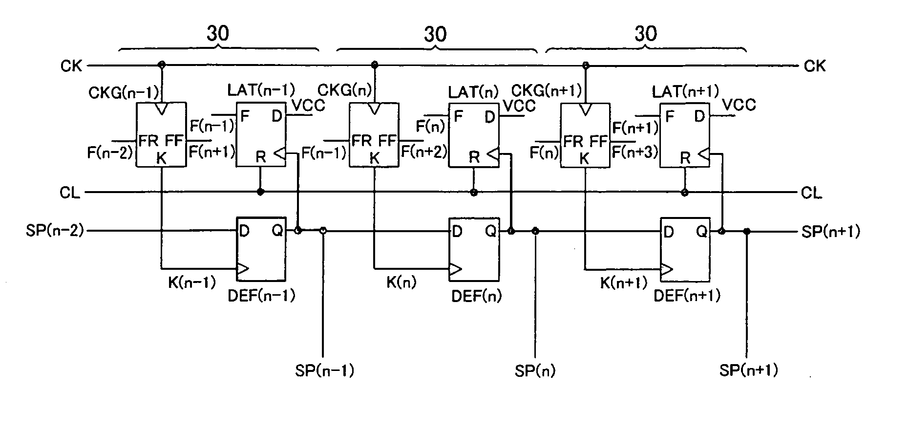
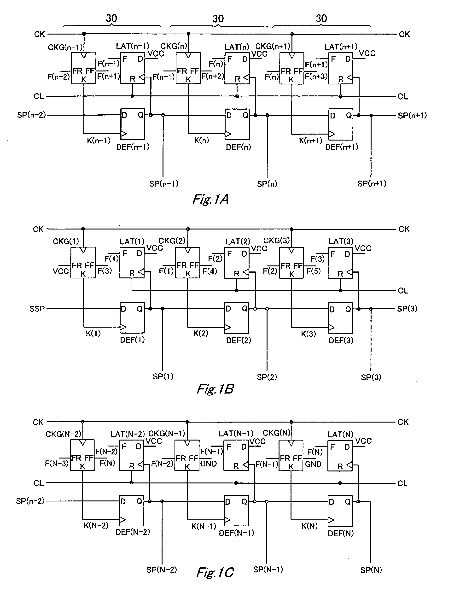
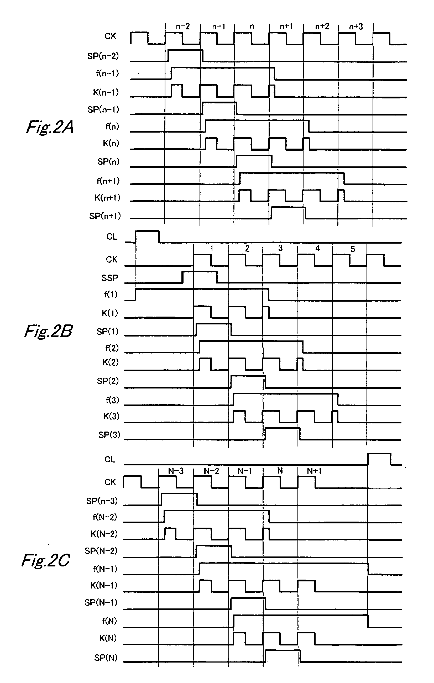
[0089]FIGS. 1A to 1C show one embodiment of a shift register of this invention, and in the same manner as in the conventional shift register of FIG. 8, it generates a group of N pieces of pulse signals. FIG. 1A shows an intermediate scanning part of the shift register, and FIG. 1B shows a start scanning part of the shift register, and FIG. 1C shows an end scanning part of the shift register.

[0090] Intermediate Scanning Part

[0091]FIG. 1A shows three units 30 of (n−1)th, (n)th and (n+1)th which were arranged arbitrarily in between.

[0092] The input clock signal CK is inputted to respective clock signal input terminals of the clock gate circuits CKG(n−1), CKG(n) and CKG(n+1).

[0093] From the extraction clock output terminal K of CKG(n−1), the clock signal K(n−1) is outputted and inputted to the extraction clock signal input terminal of the register circuit DFF(n−1), and to the D input terminal D of DFF(n−1), the pulse signal SP(n−2), which is outputted from the Q output terminal Q of...

embodiment 2

[0167]FIGS. 3A to 3C show another embodiment of a shift register of this invention, and in the same manner as in the conventional shift register of FIG. 8, it generates a group of 2N pieces of pulse signals. Unless otherwise noted, terminals, signals and the like with the same reference numerals and signs as in FIG. 1 represents ones which have the same operations and functions. In addition, in this embodiment, a pair of register circuits Da(n) and Db(n) correspond to the pulse generation portion, respectively.

[0168] Intermediate Scanning Part

[0169]FIG. 3A shows three units 30 of (n−1)th, (n)th and (n+1)th which were arranged arbitrarily in between.

[0170] The input clock signal CK is inputted to respective clock signal input terminals of the clock gate circuits CKG(n−1), CKG(n) and CKG(n+1).

[0171] From the extraction clock output terminal K of CKG (n−1), the clock signal K(n−1) is outputted and inputted to the extraction clock signal input terminals of the register circuit Da(n−...

embodiment 3

[0230]FIG. 7B shows a CKG circuit which can further reduce power consumption as compared to the CKG circuit of FIG. 7A which is used in the shift registers of the embodiments 1 and 2 which used this invention.

[0231] The clock signal input terminal CLK is inputted to an extraction switch which is configured by M9 and M10, and the other end of the extraction switch is connected to a reset switch which is configured by M11 between the other end of the switch and the ground GND, and inputted to a clock buffer circuit (clock output part) which comprises M12 to M15, and the positive clock ck and the negative clock nck are outputted.

[0232] Also, to M10 / G, the positive clock gate signal f is connected, and to M9 / G and M11 / G, the negative clock gate signal Nf is connected. Since channel capacity Cox of a MOS transistor does not function as capacity when a channel is shut off, there remains only coupling capacitance which is smaller than the channel capacity Cox between a gate and a source ...


PUM


Abstract

A shift register includes a plurality of pulse generation portions for generating a series of pulse signals in response to a level change of inputted clock signals, and a plurality of shift pulse generation units. The plurality of shift pulse generation units has a predetermined shift pulse generation unit, with the predetermined shift pulse generation unit having a status signal generation circuit for outputting a first status signal to common wiring to which both of an earlier shift pulse generation unit and a later shift pulse generation unit are connected, and a clock supply circuit for supplying a clock signal to the pulse generation portion which belongs to the predetermined shift pulse generation unit. In addition, there is a first period in which the clock supply circuit supplies the clock signal to the pulse generation portion which belongs to the predetermined shift pulse generation unit and a second period in which the clock signal is not supplied. During the first period in which the clock signal is supplied, a status signal is inputted from the earlier shift pulse generation unit, and a status signal is not inputted from the later shift pulse generation unit.

Description

BACKGROUND OF THE INVENTION [0001] 1. Field of the Invention [0002] This invention relates to a shift register which is useful for a system such as a display panel etc. which requires power saving including a shift register. [0003] 2. Description of the Related Art [0004] In an image display apparatus which was configured such that pixels with light emitting devices etc. are arranged in a two-dimensional manner, in order to generate sampling pulses for taking in input serial data (information), for example, a shift register as shown in FIG. 8 is used. This is of such a simple structure that a scanning start signal SSP and a clock signal CK are inputted, and N pieces of registers (D type flip flop (hereinafter, abbreviated as DFF)), and the clock signal CK is inputted to all clock inputs of each DFF, and a Q output of each DFF is connected to a D input of a next stage DFF, and N pieces of sampling pulses SP(1) to SP(N) from a Q output of each DFF. [0005]FIG. 9 is a time chart showing...

Claims


Application Information

Patent Timeline
Patent Type & Authority Applications(United States)
IPC IPC(8): G09G3/20H01L51/50G09G3/30G09G3/36G11C19/00G11C19/18G11C19/28
CPCG11C19/184G11C19/00
Inventor KAWASAKI, SOMEIISEKI, MASAMI
Owner CANON KK
Why Eureka
Try Eureka