Address mapping method and mapping information managing method for flash memory, and flash memory using the same

a technology of address mapping and mapping information, applied in the field of accessing flash memory, can solve the problems of insufficient achievement of large block flash memory, inability to obtain inability to achieve large block flash memory advantage, etc., to achieve the effect of maximizing the performance of the flash memory system

Active Publication Date: 2005-06-30
SAMSUNG ELECTRONICS CO LTD
View PDF11 Cites 147 Cited by
  • Summary
  • Abstract
  • Description
  • Claims
  • Application Information

AI Technical Summary

Benefits of technology

[0015] Another object of the present invention is to provide a method by which the performance of a flash memory system can be maximized and the system can be recovered even under sudden power failure through a logical-physical mapping information managing method.

Problems solved by technology

This is a primary reason for the degradation in performance of the flash memory.
However, if an existing logical-physical mapping algorithm is applied to a large block flash memory as it is, the advantage of the large block flash memory cannot be sufficiently achieved.
However, because an existing logical-physical mapping algorithm assumes that the sector size of a host is identical to the basis for the operation of the flash memory, the advantage of the large block flash memory cannot be obtained when existing algorithms are applied to the large block flash memory.
In particular, even though the large block flash memory exhibits excellent performance with respect to write operations for one or more successive sectors (multiple sector write operations), the existing algorithms do not consider such a feature.

Method used


Image

  • Address mapping method and mapping information managing method for flash memory, and flash memory using the same
  • Address mapping method and mapping information managing method for flash memory, and flash memory using the same
  • Address mapping method and mapping information managing method for flash memory, and flash memory using the same

Examples


Embodiment Construction

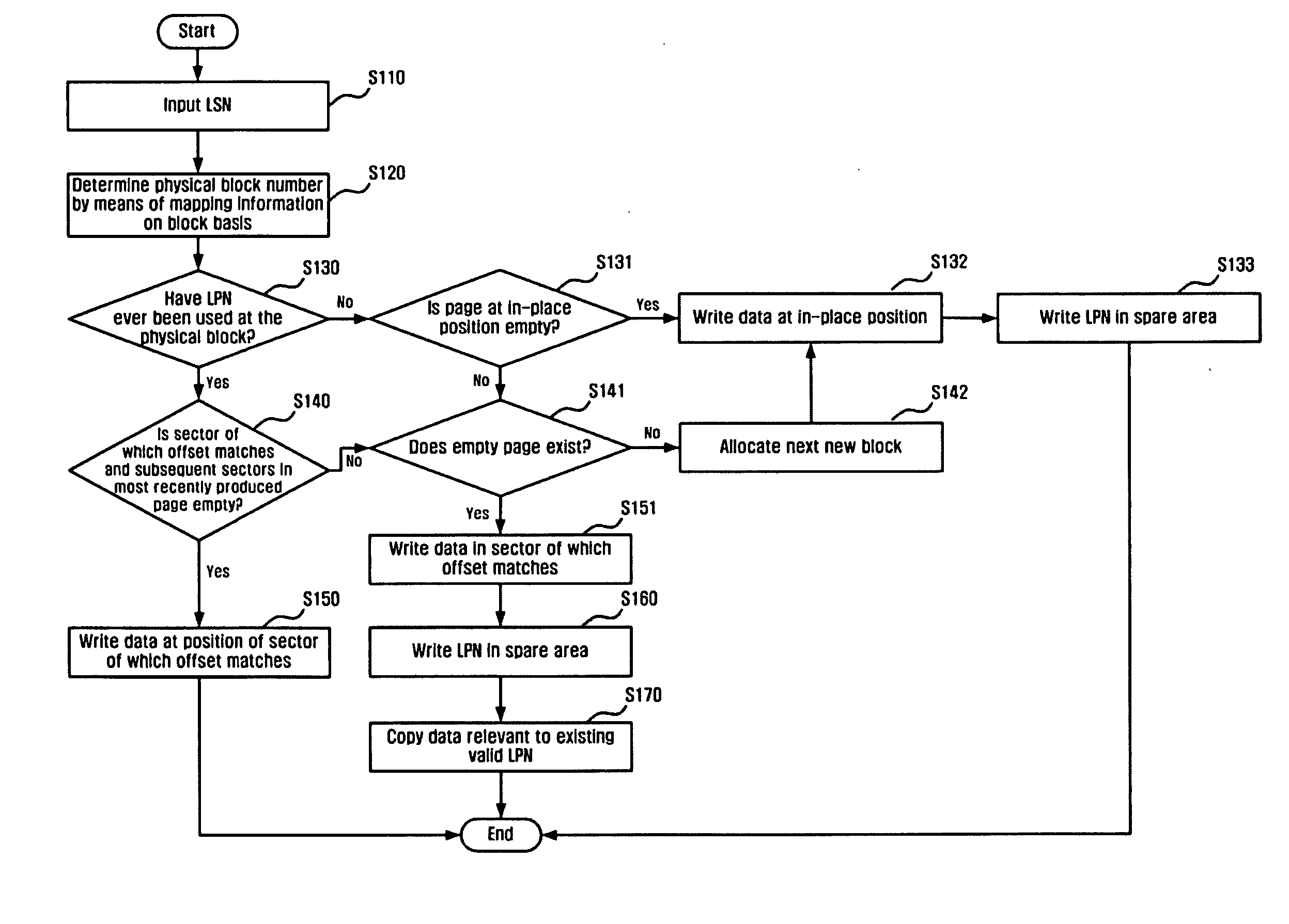
[0047] Hereinafter, exemplary embodiments of the present invention will be described in detail with respect to the accompanying drawings. The advantages and features of the present invention, and a method for achieving the advantage and features will be apparent from the embodiments discussed below in detail in connection with the accompanying drawings. However, the present invention is not limited to embodiments disclosed below and will be implemented in various different forms. The exemplary embodiments described are intended for complete disclosure of the present invention, and are provided for completely indicating the scope of the present invention to a person skilled in the art to which the present invention belongs. The present invention is only defined by the scope of the claims. Like reference numerals indicate like components throughout the description herein.

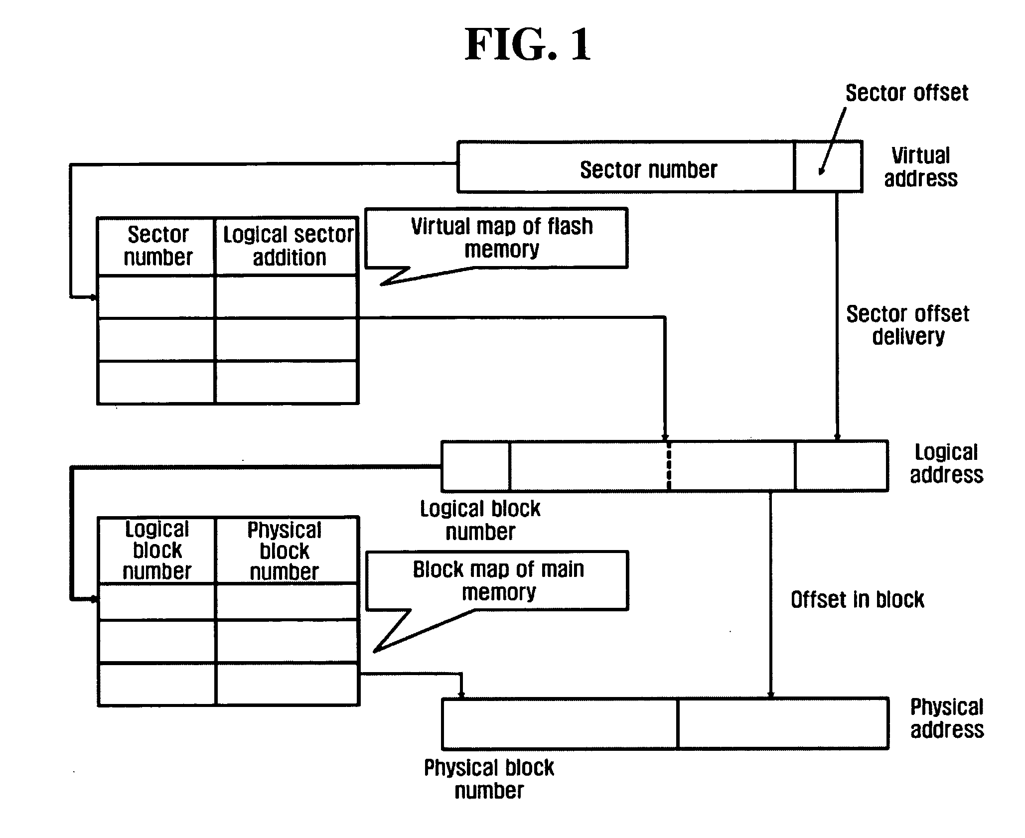
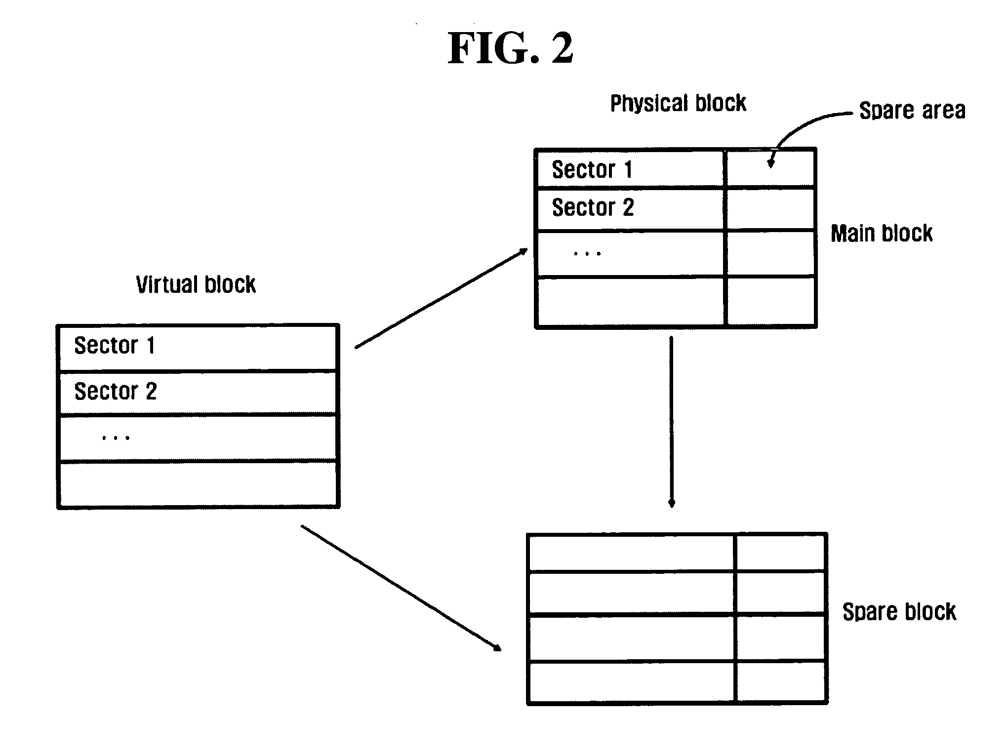
[0048]FIG. 3 illustrates an entire structure of a system with a flash memory running thereon. An XIP-able memory 3...


PUM


Abstract

A method for minimizing the degradation of performance upon accessing a flash memory using a logical-physical mapping scheme, and a method for efficiently storing and managing information on logical-physical mapping in a flash memory. A method for writing data in a flash memory includes determining whether a sector is empty in a physical page having a most recently written logical page number of data to be written, the offset of the sector matching that of the data to be written; if the sector is empty, writing the data in the sector to the physical page; and if the sector is not empty, selecting an empty physical page to write the data to a sector in the selected empty physical page of which the offset matches that of the data to be written and writing a logical page number for the data to the selected empty physical page.

Description

[0001] This application claims the priority of Korean Patent Application No. 10-2003-0100488 filed on Dec. 30, 2003, in the Korean Intellectual Property Office, the disclosure of which is incorporated herein in its entirety by reference. FIELD OF INVENTION [0002] The present invention relates to a method for accessing a flash memory, and more particularly, to a method for reducing the degradation of performance when accessing a flash memory using a logical-physical mapping scheme, and a method for efficiently storing and managing information on logical-physical mapping in a flash memory. DESCRIPTION OF THE PRIOR ART [0003] Flash memories are widely used in applications such as embedded systems and mobile devices since they have high access speed and low power consumption while being non-volatile in the same manner as hard disks. [0004] In order to perform a write operation in an already written sector of a flash memory, an operation of erasing an entire block including the sector sh...

Claims


Application Information

Patent Timeline
Patent Type & Authority Applications(United States)
IPC IPC(8): G06F12/00G06F12/06G06F12/02
CPCG06F12/0246G06F16/1847G06F12/06
Inventor CHUNG, TAE-SUNIN, JI-HYUNJUNG, MYUNG-JIN
Owner SAMSUNG ELECTRONICS CO LTD
Why Eureka
Try Eureka