Contact-connection of nanotubes

a nanotube and contact technology, applied in the direction of discharge tube main electrodes, liquid/solution decomposition chemical coatings, semiconductor/solid-state device details, etc., can solve the problems of high cost, high resistance, and inability to achieve low-resistance contact between nanotubes and interconnects at considerable cost, so as to achieve the lowest possible resistance

Inactive Publication Date: 2005-07-07
INFINEON TECH AG
View PDF12 Cites 22 Cited by
  • Summary
  • Abstract
  • Description
  • Claims
  • Application Information

AI Technical Summary

Benefits of technology

[0006] Therefore, the present invention is based on an object of providing a process for the contact-connection of nanotubes, in particular carbon nanotubes, as part of their integration in an electric circuit, which is intended on the one hand to provide the contact between nanotube a

Problems solved by technology

However, without any treatment of the nanotube/interconnect contact locations, i.e. if the nanotubes are held or deposited on the interconnect only by means of van der Waals forces, contact resistances of several hundred kiloohms (kΩ) or even up to megaohms (MΩ) are observed, making it much more difficult to use nanotubes of this type in

Method used


Image

  • Contact-connection of nanotubes
  • Contact-connection of nanotubes
  • Contact-connection of nanotubes

Examples


example

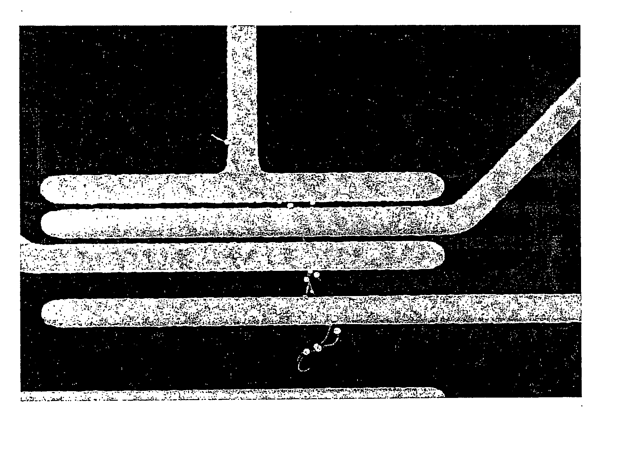
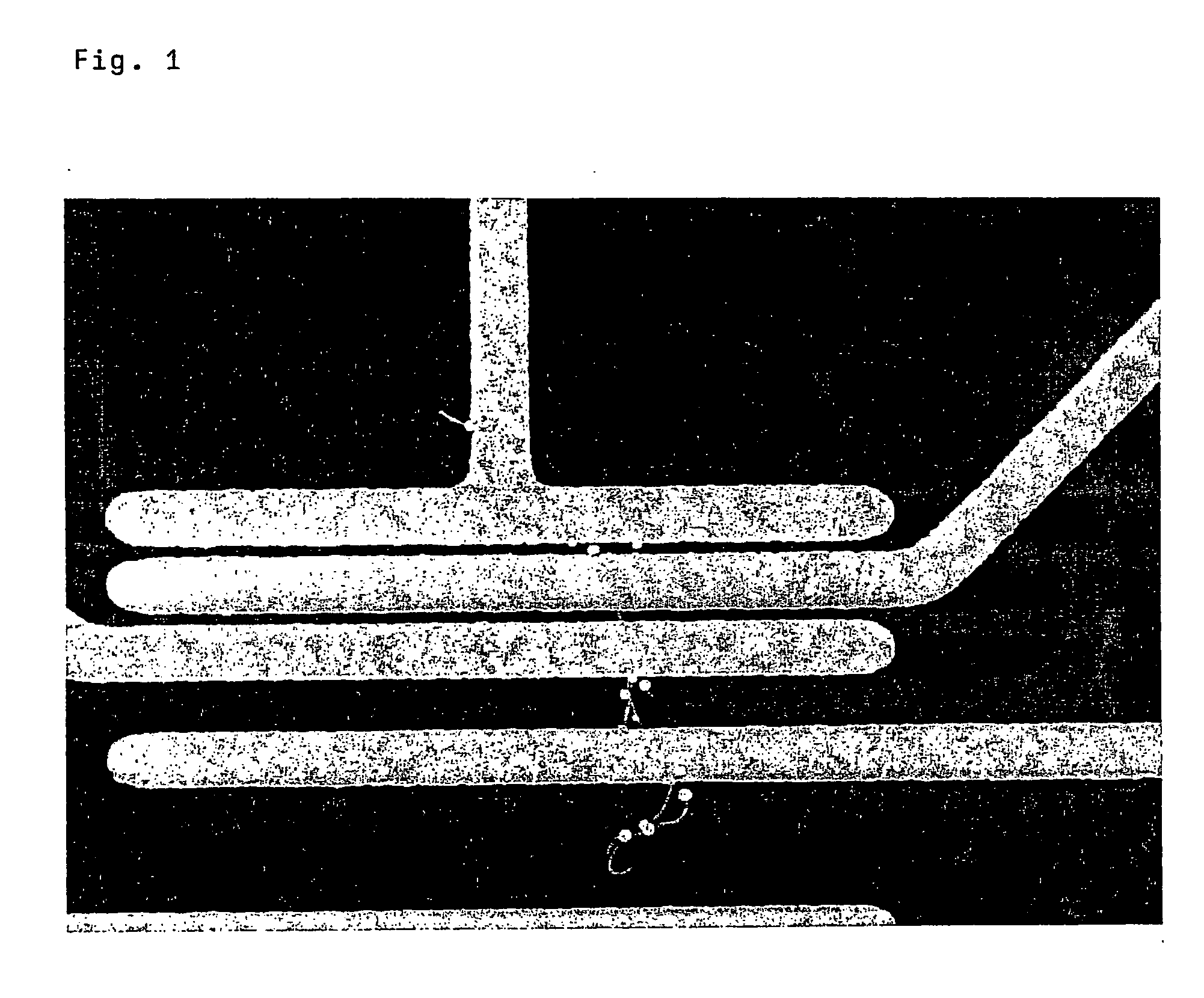
[0029] First of all, a thin (approximately 10-20 nm) iron and gold layer is applied to a silicon substrate on which there is arranged an SiO2 layer amounting to a few hundred nanometers, by means of a sputtering technique using a conventional photoresist mask which has already been pre-patterned with the predetermined contact surfaces or interconnects. Alternatively, a titanium-gold layer was also applied, and a 10 nm thick iron layer was then sputtered onto this layer. After the lift-off step, the correspondingly desired, predetermined interconnect pattern was obtained on the SiO2 surface.

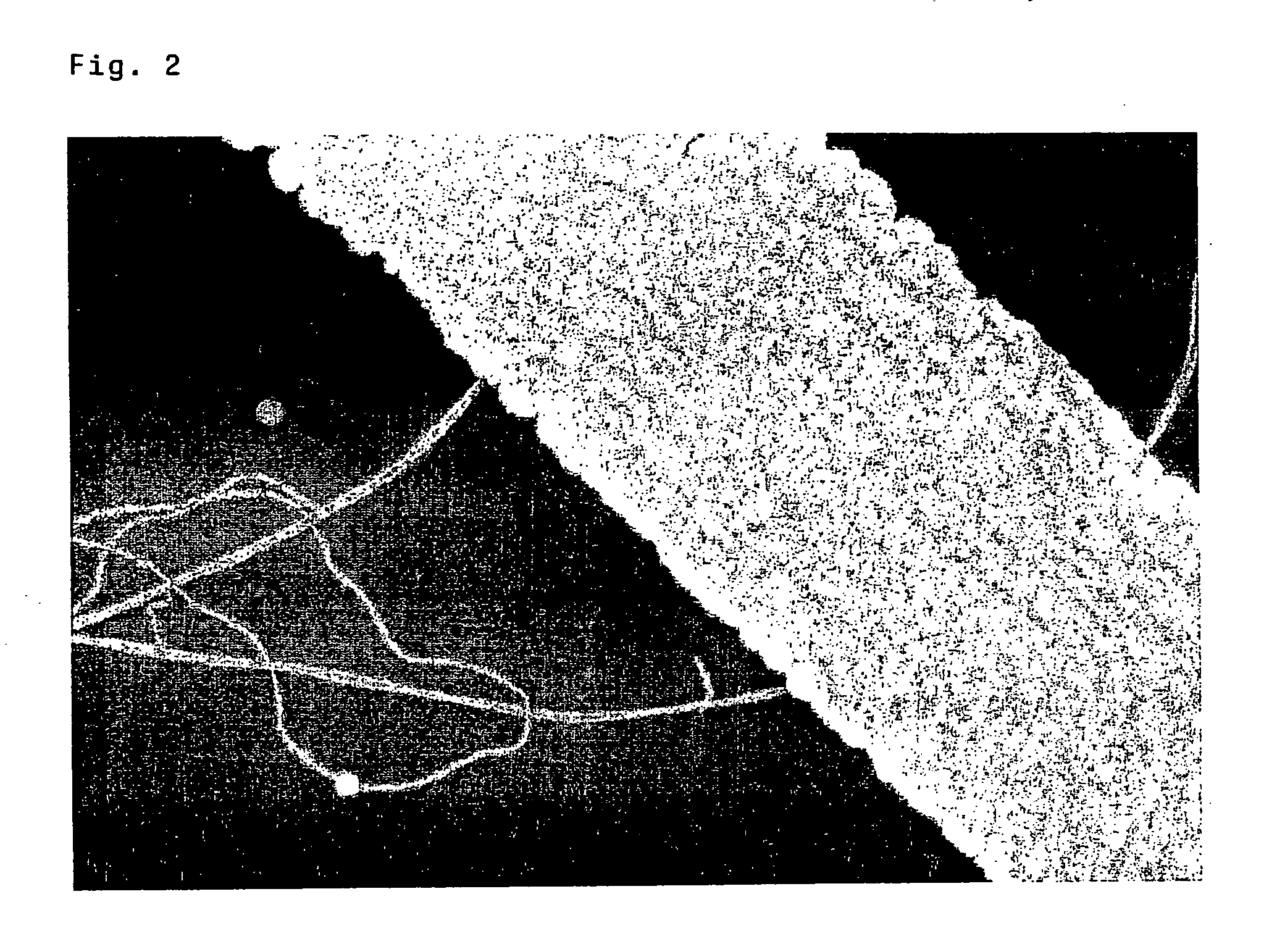
[0030] Then, a dispersion of carbon nanotubes in dimethylformamide / isopropanol was applied by spraying to the substrate which had been provided with the predetermined interconnect pattern (airbrush process).

[0031] Then, the substrate was immersed for 15 seconds in an ammoniacal metallization solution at a temperature of 85° C. which, with a pH of approximately 9, contained approximately 21 g of ...


PUM

PropertyMeasurementUnit
Contact resistanceaaaaaaaaaa
Deposition rateaaaaaaaaaa

Abstract

Process for contact-connection of carbon nanotubes as part of their integration in an electric circuit, wherein the nanotubes, after they have been applied to metallic interconnects of the electric circuit, are connected to the interconnects at contact locations by electroless metallization.

Description

CROSS-REFERENCE TO RELATED APPLICATION [0001] This application is a continuation of International Patent Application Serial No. PCT / EP2003 / 003341, filed Mar. 31, 2003, which published in German on Nov. 13, 2003 as WO 2003 / 094226, and is incorporated herein by reference in its entirety.FIELD OF THE INVENTION [0002] The present invention relates to a process for the contact-connection of nanotubes, in particular carbon nanotubes, as part of their integration in an electric circuit, wherein the nanotubes, after they have been applied to the metallic interconnects of the electric circuit, are connected to the interconnects at the contact locations by electroless metallization. BACKGROUND OF THE INVENTION [0003] On account of the fact that nanotubes, in particular carbon nanotubes, are suitable for use as metallic conductors and as semiconductors, within the context of nanocircuitry it is desirable for nanotubes of this type to be fixed to electric circuits or electronic components. The ...

Claims


Application Information

Patent Timeline
IPC IPC(8): C23C18/16H01L21/288H01L23/522H01L23/532H01L51/30
CPCB82Y10/00H01L21/288H01L23/522H01L23/53276H01L51/0048H01L2924/0002C23C18/1662H01L2924/00H10K85/221
Inventor UNGER, EUGENDUSBERG, GEORG S.KREUPL, FRANZGRAHAM, ANDREWLIEBAU, MAIK
Owner INFINEON TECH AG
Why Eureka
Try Eureka