Method for fabricating a bipolar transistor

a technology of bipolar transistors and fabrication methods, which is applied in the direction of basic electric elements, electrical apparatus, and semiconductor devices, can solve the problems of high process engineering complexity, unusable transistors, and high cost, and achieve the effect of keeping the number of process steps as low

Inactive Publication Date: 2005-02-15
INFINEON TECH AG
View PDF17 Cites 5 Cited by
  • Summary
  • Abstract
  • Description
  • Claims
  • Application Information

AI Technical Summary

Benefits of technology

Therefore, the present invention is based on the object of providing a method for fabricating a bipolar transistor, which does not have the difficulties whic

Problems solved by technology

However, to further increase the switching speed, a number of difficulties still have to be eliminated.
These undesired layers may cause a short circuit between the emitter and the collector, to make the transistor unusable.
However, a drawback of this method is th

Method used


Image

  • Method for fabricating a bipolar transistor
  • Method for fabricating a bipolar transistor
  • Method for fabricating a bipolar transistor

Examples


second embodiment

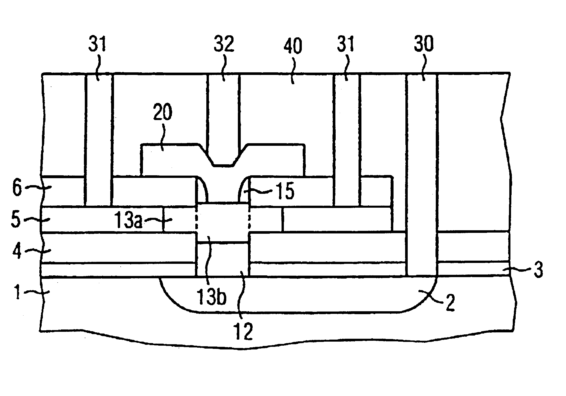
FIGS. 5A and 5B show two steps of a further inventive method, which likewise deviate from the method illustrated in FIGS. 3A to 3E. The first steps of this further inventive method are illustrated in FIG. 3A. Then, a thermal oxide layer or an oxide deposition 3, a nitride layer 4, a polysilicon layer 5 (together with p-implantation) and an oxide layer 6 are applied to the substrate as in the previous embodiment. This is followed by the production of the mask 7, then the anisotropic etching of oxide layer 6 and polysilicon layer 5, which is patterned as in the previous embodiment. Then, as in the present invention, oxidation takes place at the side wall of the polysilicon layer 5, this oxidation to some extent eating into the polysilicon.

Then, the oxide layer of the side wall of the polysilicon layer 5 is removed selectively with respect to the polysilicon of the conductive layer 5 before the production of the collector or before the etching of the nitride layer 4. Next, the nitride ...

first embodiment

Since in this way the oxide layer has already been removed at the side wall of the polysilicon layer 5, it is now possible for collector 12 and base 13 to be produced epitaxially in one step in accordance with the present invention. The resulting situation is shown in FIG. 5B. The following steps for production of the npn bi-polar transistor are then once again as described in connection with FIGS. 3D and 3E.


PUM


Abstract

A method for producing bipolar transistors with the aid of selective epitaxy for producing a collector and base. The method includes widening the area of the base either by the isotropic etching of the conductive layer or by the oxidation of the conductive layer and by the subsequent removal of the oxide layer. This widening of the area of the base prevents the occurrence of short-circuits between the emitter and the collector during the subsequent production of the base.

Description

BACKGROUND OF THE INVENTIONThe invention relates to a method for fabricating bipolar transistors, as can be used, for example, in radio frequency technology.Bipolar transistors are the transistors of choice where high switching speeds and / or high output powers are required. Modern bipolar transistors can be operated at frequencies of 50 GHz and above. However, to further increase the switching speed, a number of difficulties still have to be eliminated. Parameters, which limit the frequency, are, in particular, the parasitic capacitance between the collector and the base and the base resistance. It has been possible to reduce both parameters to an ever increasing extent by miniaturization, which has been made possible by methods such as self-aligning of the base and the emitter, LOCOS process step sequences, trench techniques and refined layer techniques, such as selective epitaxy.A further improvement is provided by bipolar transistors with hetero junctions. Bipolar transistors wit...

Claims


Application Information

Patent Timeline
IPC IPC(8): H01L21/331H01L21/02
CPCH01L29/66287
Inventor MULLER, KARL-HEINZWOLF, KONRAD
Owner INFINEON TECH AG
Why Eureka
Try Eureka