Capacitive touchpad and method for forming the same

a capacitive touchpad and capacitive technology, applied in the field of capacitive touchpad and a method for forming the same, can solve the problems of limiting the application of electronic products the electrical performance of such capacitive touchpads is much poorer than that of one, and the manufacturing cost of such capacitive touchpads is relatively high. to achieve the effect of reducing the cost of capacitive touchpads

Inactive Publication Date: 2005-07-21
ELAN MICROELECTRONICS CORPORATION
View PDF13 Cites 93 Cited by
  • Summary
  • Abstract
  • Description
  • Claims
  • Application Information

AI Technical Summary

Benefits of technology

[0005] One object of the present invention is to provide a capacitive touchpad constructed with a membrane and a PCB, and a method to p

Problems solved by technology

However, the manufacturing cost of such capacitive touchpad is relatively high.
Unfortunately, the electrical performance of such capacitive touchpad is much poorer than that of one based on four-layer PCB, a

Method used


Image

  • Capacitive touchpad and method for forming the same
  • Capacitive touchpad and method for forming the same
  • Capacitive touchpad and method for forming the same

Examples


first embodiment

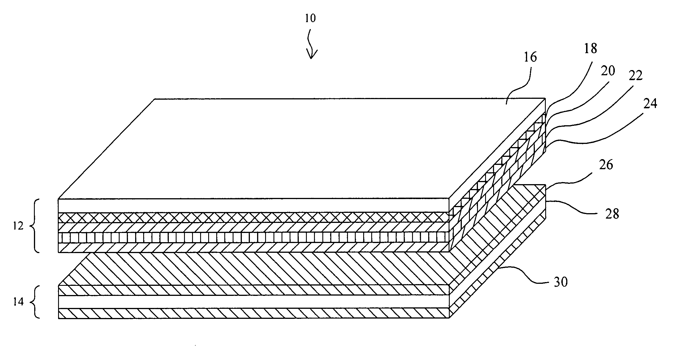
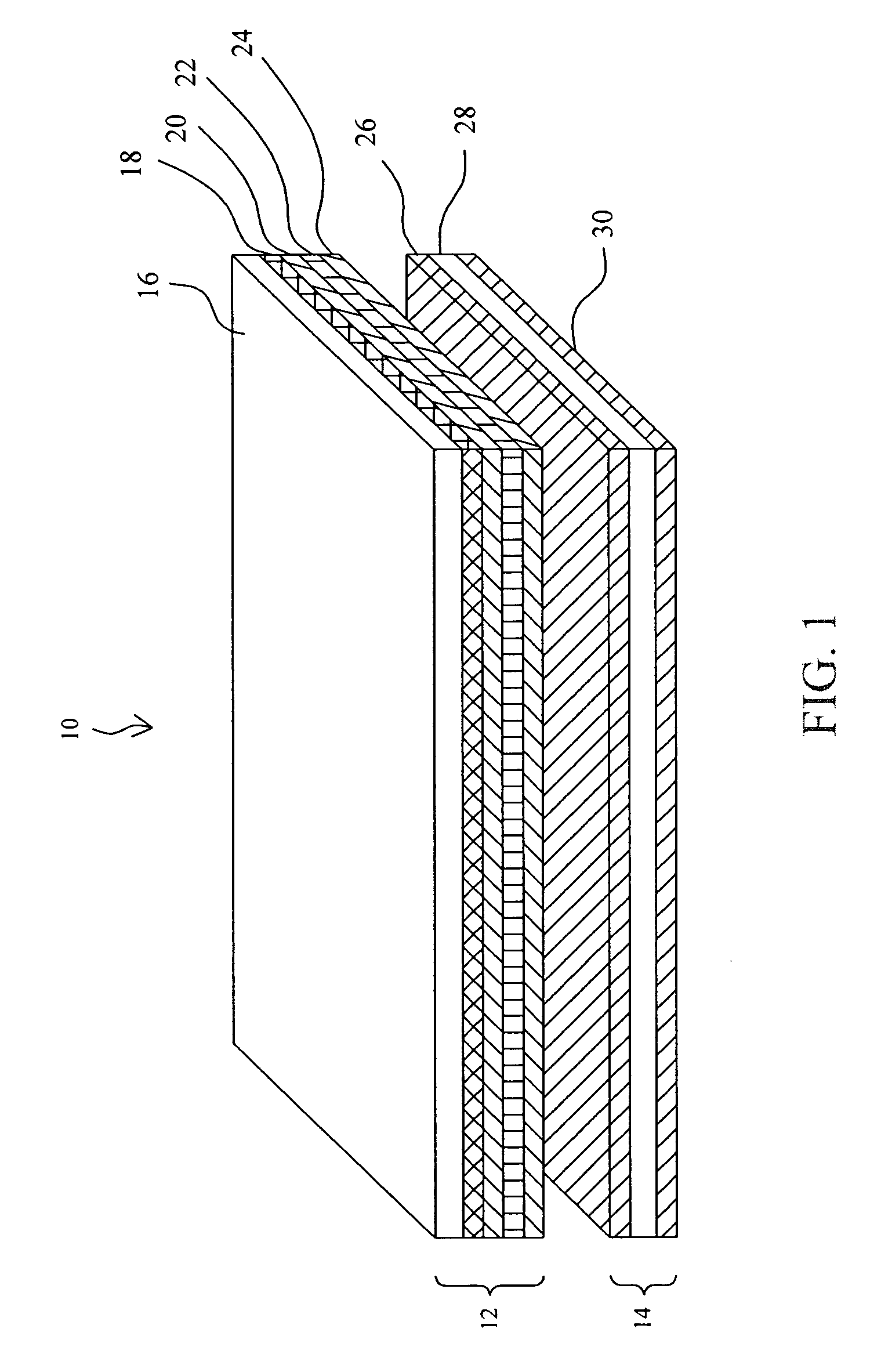
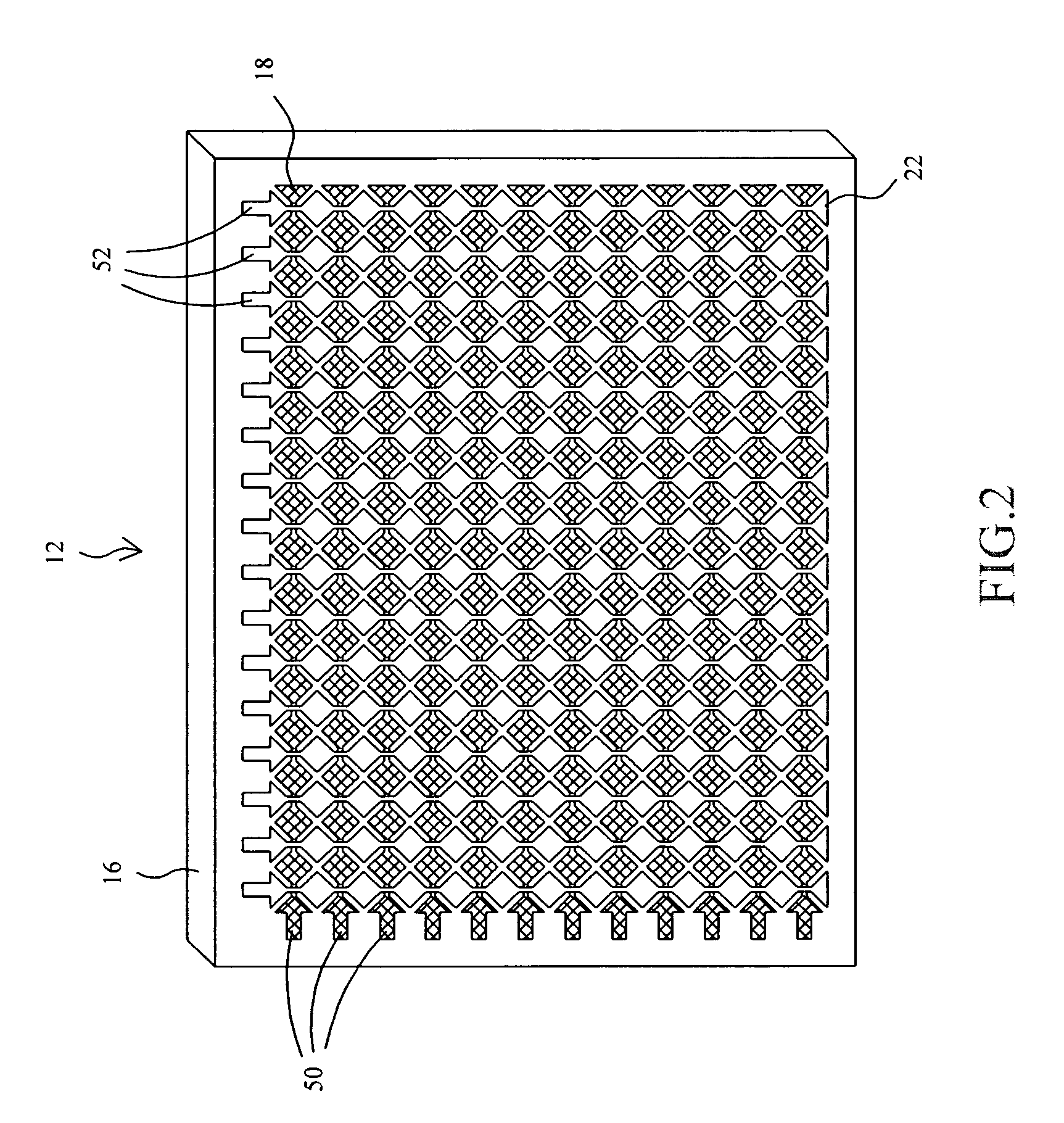
[0016]FIG. 1 shows a diagram to illustrate the structure of a first embodiment capacitive touchpad 10 that comprises a membrane 12 and a PCB 14 combined together. The membrane 12 is served as the analog sense apparatus of the capacitive touchpad 10, and constructed with sandwich structure including a first insulator layer 16, a first conductor layer 18, a second insulator layer 20, a second conductor layer 22, and a third insulator layer 24 sequentially in stack. The insulator layer 16 is used as the substrate of the membrane 12, and may be made of transparent insulator such as polyester (PET), or opaque insulator such as plastic, ceramic and polymer. The Y trace of the capacitive touchpad 10 is included in the conductor layer 18, the X trace is included in the conductor layer 22, and both of them are made of material with low resistance, for example silver glue. The insulator layer 20 provides the insulation between the conductor layers 18 and 22, and the insulator layer 24 is for ...

second embodiment

[0020]FIG. 4 shows a diagram to illustrate the structure of a second embodiment capacitive touchpad 200 that also comprises a membrane 202 and a PCB 204, and also employs the membrane 202 served as the analog sense apparatus, while the membrane 12 is constructed with four-layer sandwich including a first insulator layer 206, a first conductor layer 208, a second insulator layer 210 and a second conductor layer 212 sequentially in stack. The insulator layer 206 may be made of transparent insulator such as PET, or opaque insulator such as plastic, ceramic and polymer. The Y trace of the capacitive touchpad 200 is included in the conductor layer 208, the X trace is included in the conductor layer 212, and both of them are made of material with low resistance, for example silver glue. The insulator layer 210 providing the insulation between the conductor layers 208 and 212 has dielectric constant of 2-4, and may be made of transparent insulator such as ink, or opaque insulator such as p...


PUM


Abstract

A capacitive touchpad comprises a membrane and a printed circuit board combined together. The membrane comprises an X trace and a Y trace with an insulator layer inserted therebetween, and the printed circuit board has connection pads on a top side of a substrate that are electrically connected to the X and Y traces. The printed circuit board further comprises vias connected between the connection pads and a conductor layer on the bottom side of the substrate. To form the capacitive touchpad, the membrane and printed circuit board are individually produced in advance, and then combined together. Alternatively, the membrane is printed on the printed circuit board.

Description

FIELD OF THE INVENTION [0001] The present invention is related generally to a capacitive touchpad and a method for forming the capacitive touchpad, and more particularly, to a capacitive touchpad including a membrane thereof and a method for forming the capacitive touchpad. BACKGROUND OF THE INVENTION [0002] Touchpad has found wide applications in various electronic products, and conventionally, there are three types of touchpad, i.e., resistive, electromagnetic, and capacitive ones. Theoretically, the capacitive touchpad determines the position that is touched by finger or conductor by sensing the instant capacitance change resulted from the touch of the finger or conductor. Typically, a conventional capacitive touchpad is constructed with four-layer printed circuit board (PCB), including a ground plane, an X trace, a Y trace, and a layer of circuit. However, the manufacturing cost of such capacitive touchpad is relatively high. [0003] For cost down, it was proposed a capacitive to...

Claims


Application Information

Patent Timeline
IPC IPC(8): H01H13/00G06F3/00G06F3/044G09G5/00H01H11/00
CPCG06F3/044G06F3/0445G06F3/0446A01C1/02
Inventor CHIU, YEN-CHANGCHIEN, YUNG-LIEH
Owner ELAN MICROELECTRONICS CORPORATION
Why Eureka
Try Eureka