Method and circuit for writing double data rate (DDR) sampled data in a memory device

a memory device and data sample technology, applied in the field of memory devices, can solve the problems of insufficient holding margin, insufficient setup margin mb>1/b>, error upon writing data, etc., and achieve the effect of maximizing the operation speed of the semiconductor memory device, sufficient setup, and holding margins

Inactive Publication Date: 2005-07-21
SAMSUNG ELECTRONICS CO LTD
View PDF10 Cites 17 Cited by
  • Summary
  • Abstract
  • Description
  • Claims
  • Application Information

AI Technical Summary

Benefits of technology

[0019] Another aspect of the present invention provides a method for sampling data in a semiconductor memory device and a data sampling circuit therefor capable of maximizing an operation speed of the semiconductor memory device since an internal error generated upon setup and hold can be reduced or minimized by sampling the data with a path control signal synchronized with a falling edge of an external clock signal to secure sufficient setup and hold margins in all operation modes.

Problems solved by technology

The data to be written to the memory cells is changed from the first data D1_H to the second data D1_L on the first path1 and from the second data D1_L to the third data D2_H on the second path2 at a time point where the write clock signal WCLK is generated, resulting in an insufficient hold margin which may cause an error upon writing data.
As a result, there is a problem that a sufficient setup margin M1 cannot be secured because the second data D1_L on the second path Path2 is positioned at a point of ¼ or less of the external clock cycle period when the write clock signal WCLK I is generated.
Thus, there can arise a problem that an error is caused upon writing data because a setup margin in a CA mode is insufficient.
The problem is great where the SRAM device has a high operation frequency and data on the first and second paths are delayed and then used to secure the hold margin in the above-stated CC mode.

Method used


Image

  • Method and circuit for writing double data rate (DDR) sampled data in a memory device
  • Method and circuit for writing double data rate (DDR) sampled data in a memory device
  • Method and circuit for writing double data rate (DDR) sampled data in a memory device

Examples


Embodiment Construction

[0030] Preferred embodiments of the present invention will be described in detail with reference to the accompanying drawings. Descriptions in various embodiments are shown and provide examples to those skilled in the art to convey a more thoroughly understanding the present invention, and accordingly should be not construed to limit the scope of the present invention which is defined in the claims.

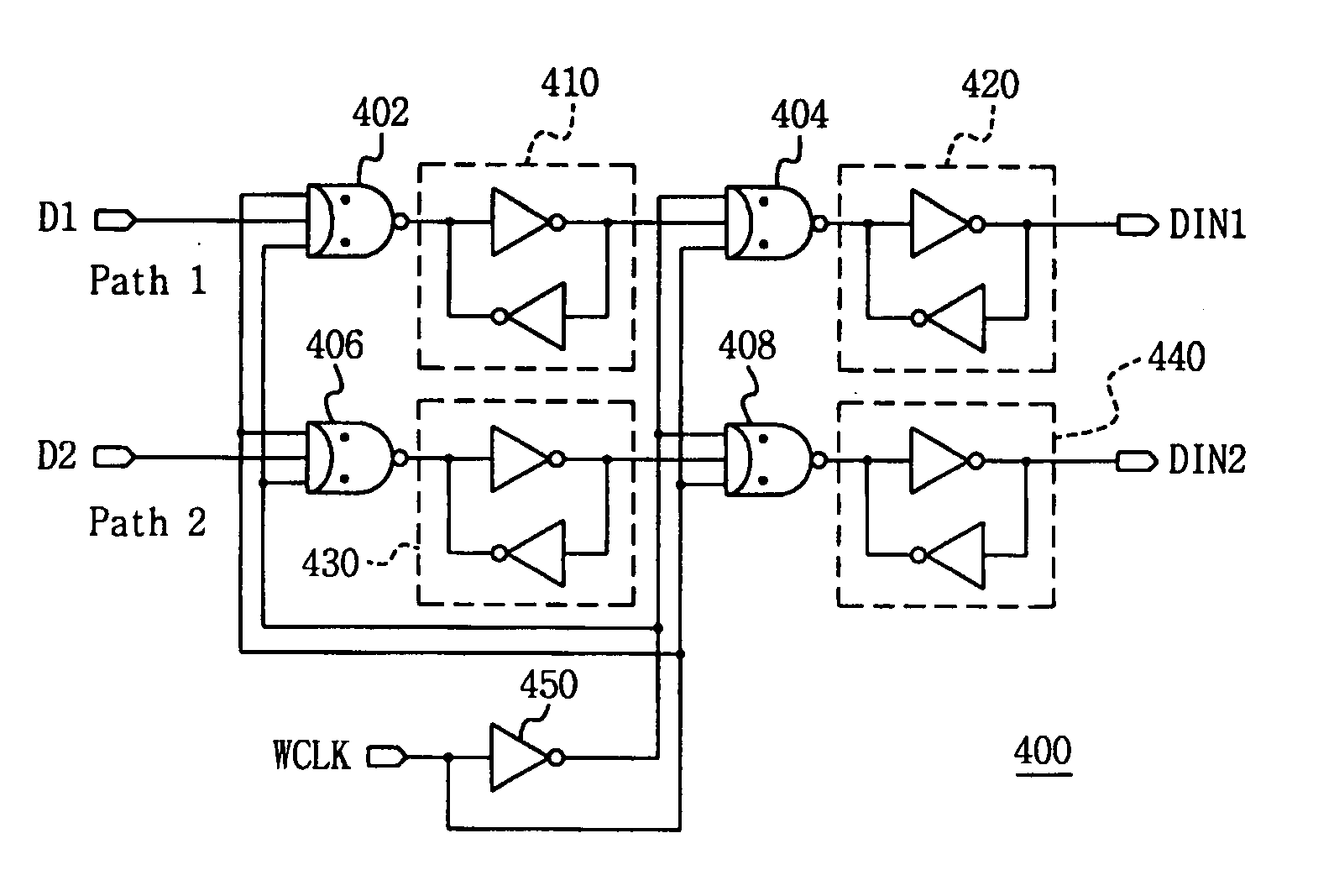
[0031]FIGS. 4, 5 and 6 are circuit diagrams showing a data sampling circuit in a DDR SRAM device according to an embodiment of the present invention. The circuit will be described specifically with reference to FIGS. 4, 5 and 6.

[0032] Referring to FIGS. 4, 5 and 6, a data sampling circuit according to an embodiment of the present invention includes a path control signal generating circuit 200 (FIG. 4), a path control circuit 300 (FIG. 5), and a write control circuit 400 (FIG. 6). As shown in FIG. 4, the path control signal generating circuit 200 includes: a first inverter 212 for invert...


PUM


Abstract

A method and circuit for sampling and writing data in a double data rate (DDR) memory device, capable of securing sufficient setup and hold margins regardless of the operation frequency. Transferring first and second sampled input data to a first path using a first path control signal. Transferring third and fourth sampled input data to a second path using a second path control signal. The first and second path control signals are one half-cycle out of phase. First to fourth data are successively sampled in synchronization with a rising or falling edge of a first external clock signal; The sampled first data is linked onto a first path and the sampled second data is linked onto a second path in response to the first path control signal (generated in synchronization with a falling edge of the external clock signal); the first data on the first path and the second data on the second path are written to the memory cells in response to a write clock signal.

Description

CROSS-REFERENCE TO RELATED APPLICATION [0001] This application claims the benefit of Korean Patent Application No. 2004-4208, filed on Jan. 20, 2004, the disclosure of which is hereby incorporated herein by reference in its entirety. BACKGROUND [0002] 1. Technical Field [0003] The present invention relates to memory devices, and more specifically, to a method and circuit for writing sampled input data to memory cells in a semiconductor memory device having a double data rate (DDR) scheme. [0004] 2. Discussion of the Related Art [0005] As the demand for higher speed semiconductor devices increases, a double data rate data sampling scheme (hereinafter, referred to as “DDR”) that is capable of inputting (writing) or outputting (reading) data at a rising edge as well as a falling edge of an external clock signal, is being increasingly employed. Data is sampled to allow two data to be read or written during one external clock cycle. Thus, Double Data Rate (DDR) is achieved by using both ...

Claims


Application Information

Patent Timeline
Patent Type & Authority Applications(United States)
IPC IPC(8): G11C7/10G11C11/417G11C11/40H04L7/00
CPCG11C7/1072G11C7/1093G11C7/1087G11C7/1078G11C7/1096G11C7/222G11C11/413
Inventor YOON, YONG-JINLEE, JONG-CHEOLCHO, UK-RAE
Owner SAMSUNG ELECTRONICS CO LTD
Why Eureka
Try Eureka