

Detector remodulator and optoelectronic switch
- Summary
- Abstract
- Description
- Claims
- Application Information
AI Technical Summary
Benefits of technology
Problems solved by technology
Method used
Image

Examples
Embodiment Construction
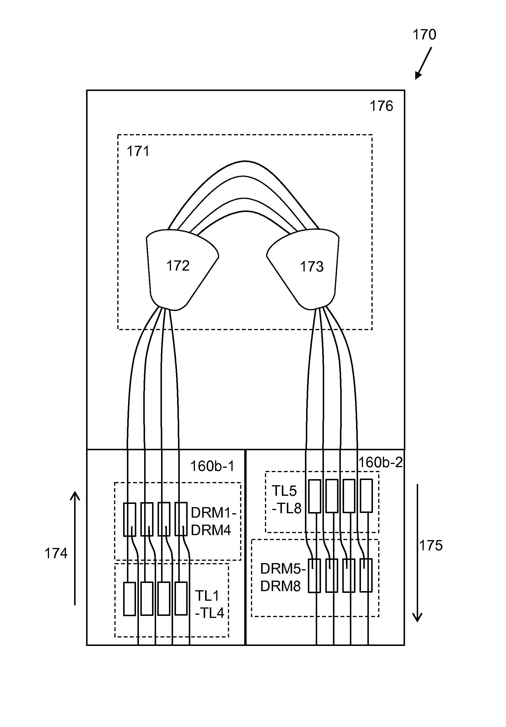
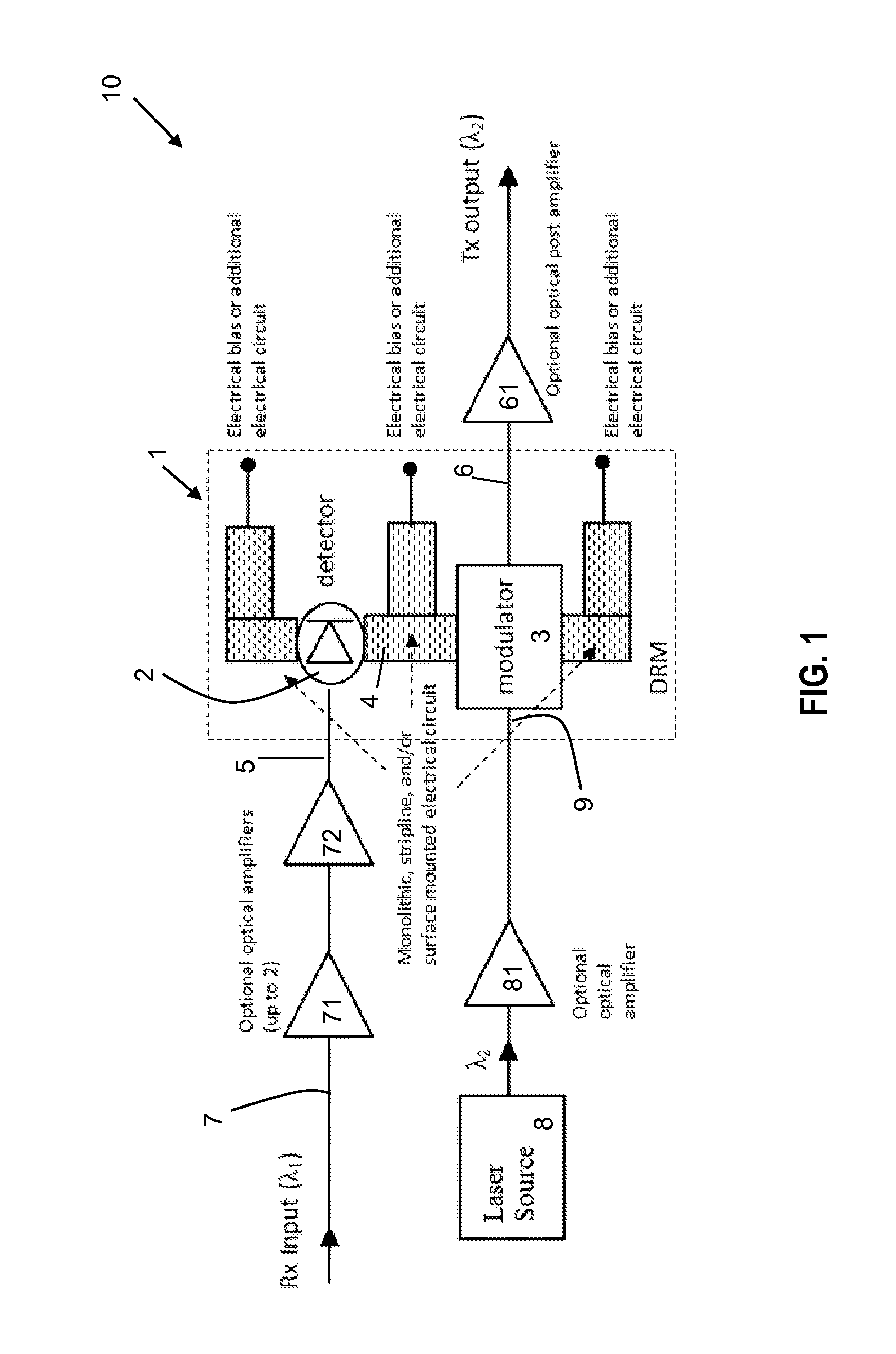
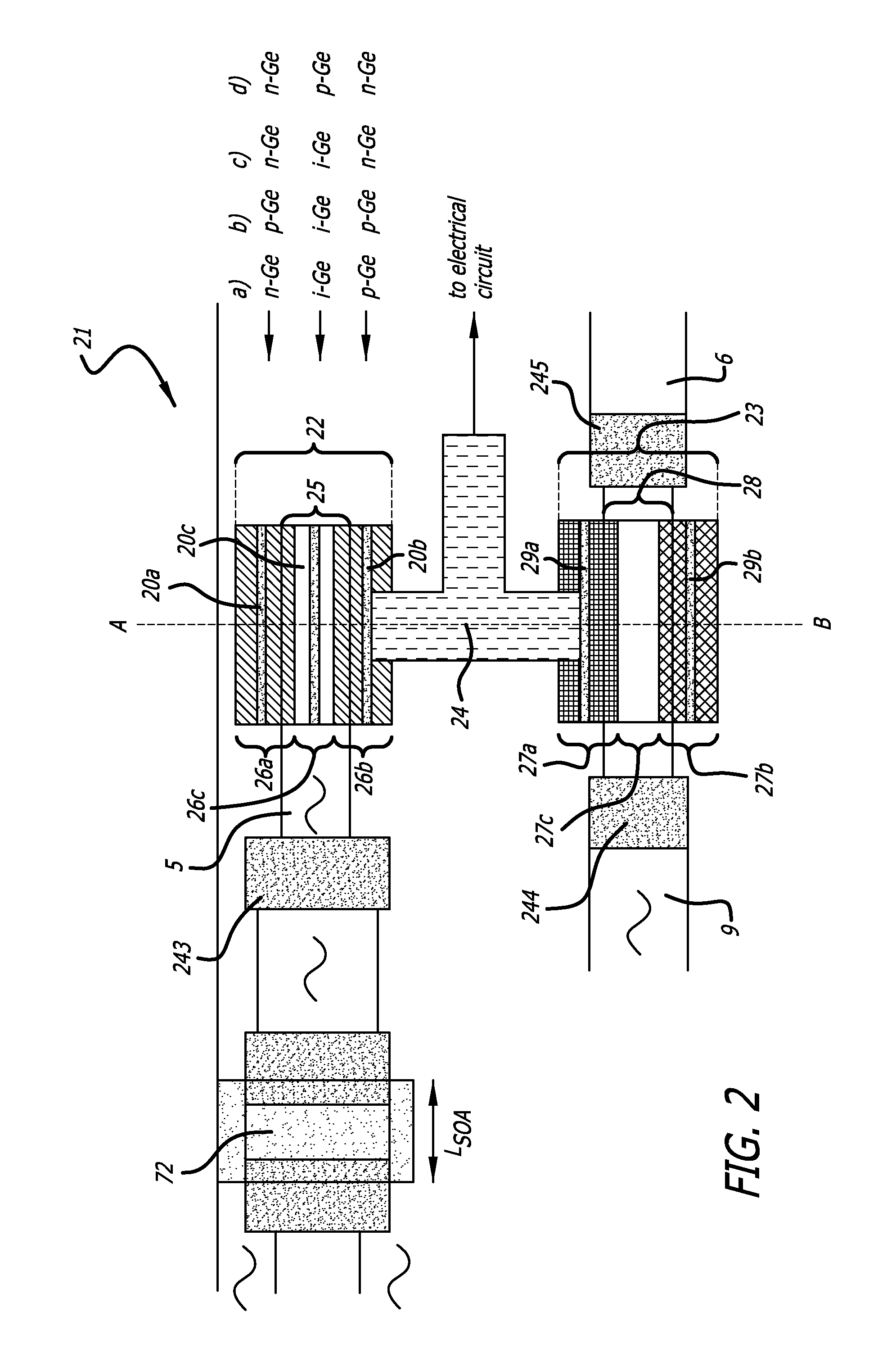
[0187]FIG. 1 shows a conversion chip 10 including a detector remodulator (DRM) 1. The detector remodulator 1 comprises a silicon on insulator (SOI) waveguide platform which includes: a detector 2, a modulator 3 and an electrical circuit 4 which electrically connects the detector to the modulator. The detector 2 is coupled to an input waveguide 5 and the modulator 3 is coupled to an output waveguide 6.
[0188]The detector 2, modulator 3, input waveguide 5 and output waveguide 6 are arranged within the same horizontal plane as one another within the SOI waveguide platform. In the embodiment shown, a portion of the electrical circuit is located directly between the detector and the modulator.
[0189]The conversion chip includes a waveguide for a (modulated) first optical signal 7 of a first wavelength λ1. In the embodiment shown in FIG. 1, the waveguide is coupled to the input waveguide 5 of the detector 2 via a first and second optical amplifier 71, 72, although in an alternative embodime...
PUM
 Abstract
Description
Claims
Application Information