
Method and circuit for writing double data rate (DDR) sampled data in a memory device
a memory device and data sample technology, applied in the field of memory devices, can solve the problems of insufficient holding margin, insufficient setup margin mb>1/b>, error upon writing data, etc., and achieve the effect of maximizing the operation speed of the semiconductor memory device, sufficient setup, and holding margins
- Summary
- Abstract
- Description
- Claims
- Application Information
AI Technical Summary
Benefits of technology
Problems solved by technology
Method used
Image

Examples
Embodiment Construction
[0030]Preferred embodiments of the present invention will be described in detail with reference to the accompanying drawings. Descriptions in various embodiments are shown and provide examples to those skilled in the art to convey a more thoroughly understanding the present invention, and accordingly should be not construed to limit the scope of the present invention which is defined in the claims.
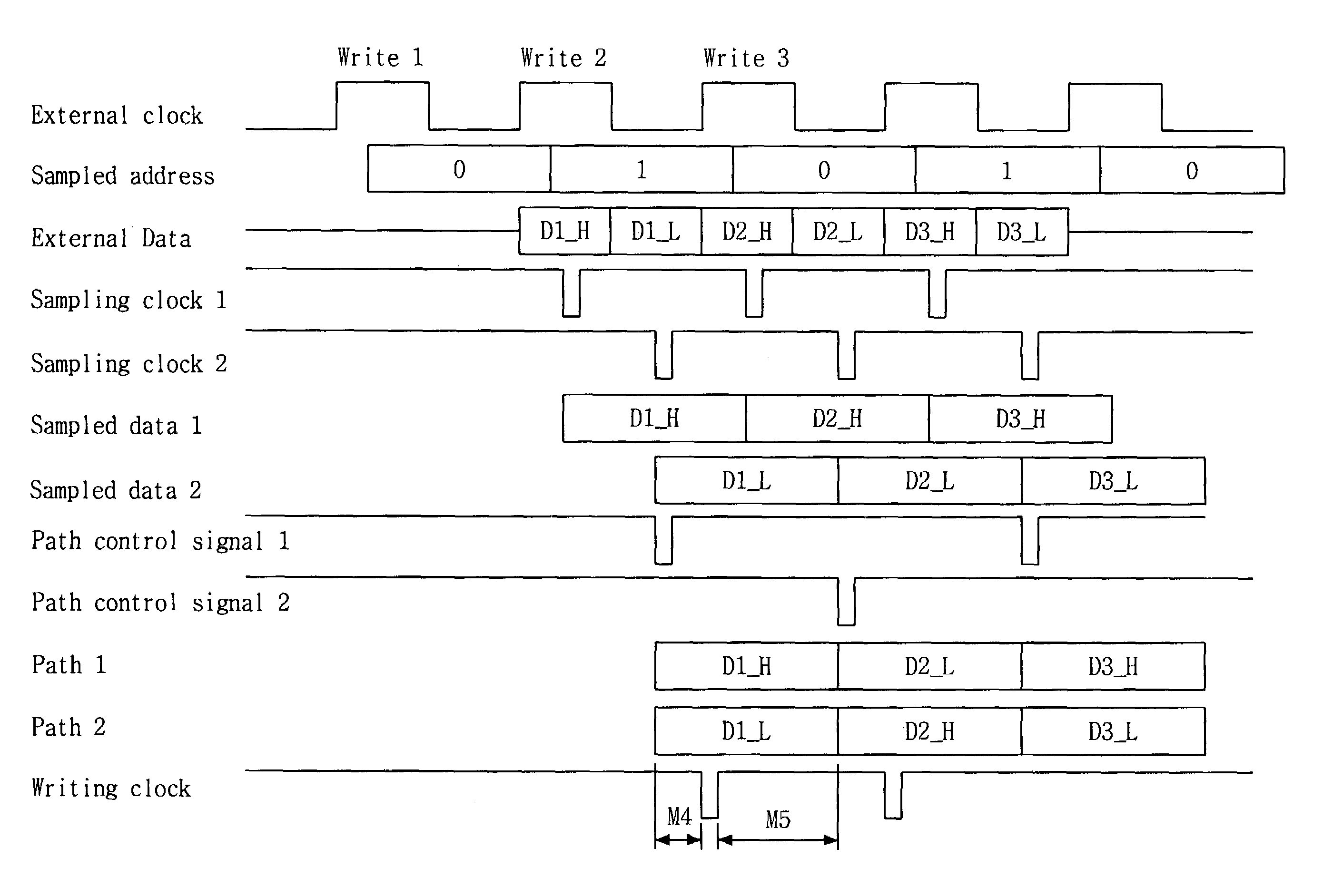
[0031]FIGS. 4, 5 and 6 are circuit diagrams showing a data sampling circuit in a DDR SRAM device according to an embodiment of the present invention. The circuit will be described specifically with reference to FIGS. 4, 5 and 6.
[0032]Referring to FIGS. 4, 5 and 6, a data sampling circuit according to an embodiment of the present invention includes a path control signal generating circuit 200 (FIG. 4), a path control circuit 300 (FIG. 5), and a write control circuit 400 (FIG. 6). As shown in FIG. 4, the path control signal generating circuit 200 includes: a first inverter 212 for inverting ...
PUM
 Abstract
Description
Claims
Application Information