Method for making film assembly used in PDP filter, film assembly manufactured by the method, and PDP filter with the film assembly
a technology of film assembly and filter, which is applied in the manufacture of discharge tube/lamp details, tube/lamp screen manufacturing, and non-electron-emitting shielding screens, etc. it can solve the problems of degrading productivity, inability to manufacture large quantities of film assembly partially constituting the pdp filter, and inability to meet the requirements of filtration and filtering
- Summary
- Abstract
- Description
- Claims
- Application Information
AI Technical Summary
Benefits of technology
Problems solved by technology
Method used
Image
Examples
first embodiment
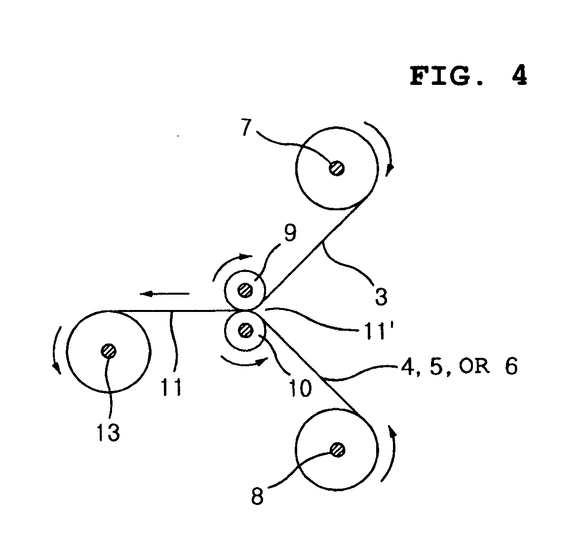
[0049]FIG. 4 shows the arrangement of roller apparatuses used to manufacture a film assembly for a PDP filter according to the present invention and FIG. 5 is a flowchart showing a method for manufacturing a film assembly for a PDP filter according to the present invention.
[0050] A method for manufacturing a film assembly for a PDP filter according to a first embodiment of the present invention will now be described with reference to FIGS. 5 to 9.
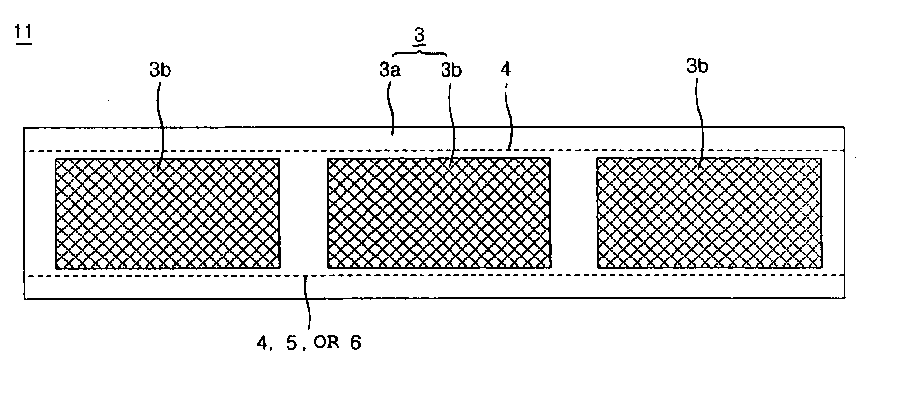
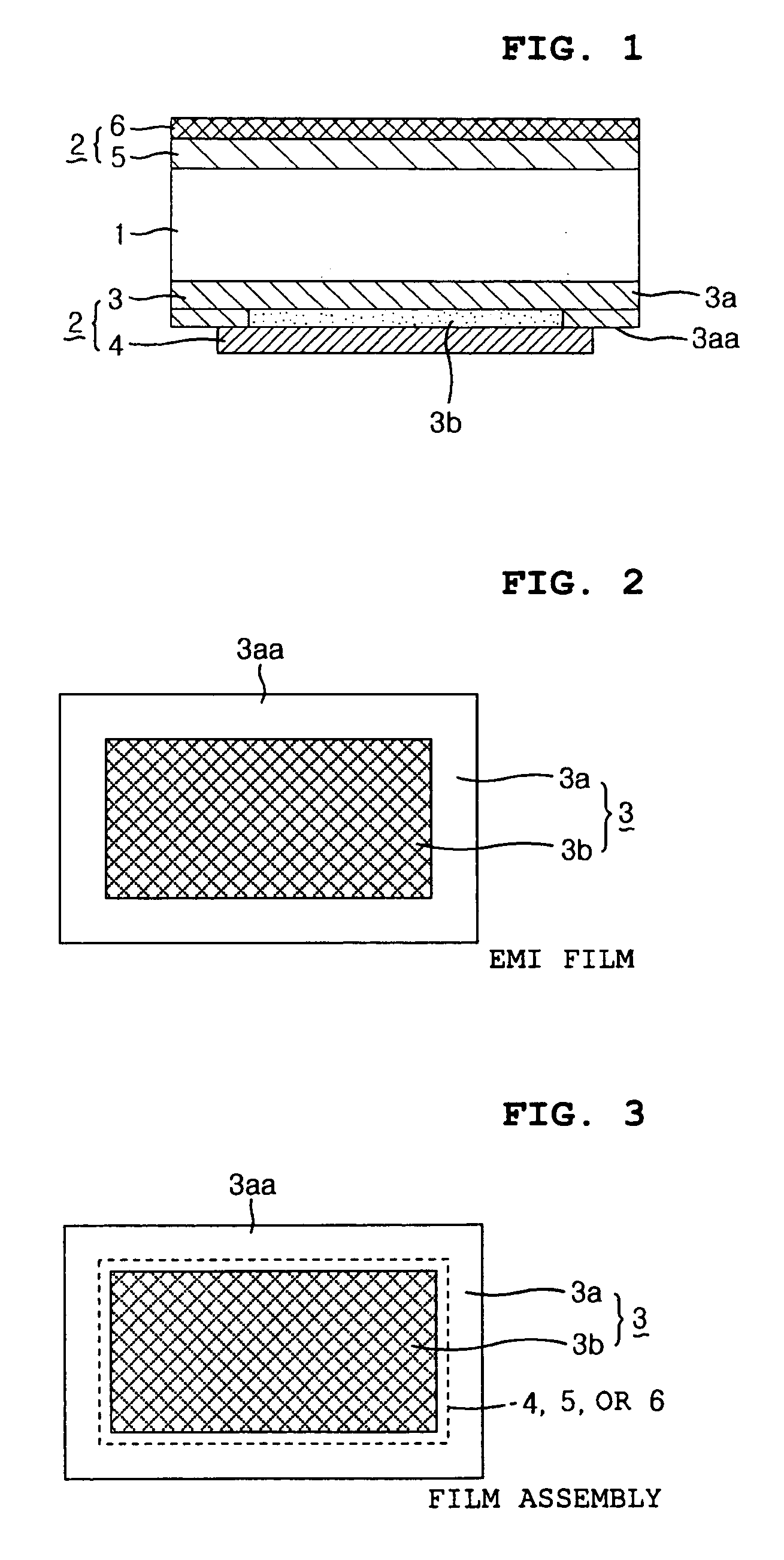
[0051] An EMI film 3 having a number of conductive effective screen portions 3b formed on a surface of a long transparent polymer resin film 3a with a predetermined spacing is provided in a roll type. The wound roll of the EMI film is then mounted on a first feed roller 7 (step 500).
[0052] Next, at least one long transparent functional film 4, 5, and 6 capable of covering at least partially the effective screen portions 3b of the EMI film 3 is provided in a roll type. The wound roll of the functional film is then mounted on a second feed ...
second embodiment
[0100]FIG. 15 is a sectional view showing a PDP filter according to the present invention. The PDP filter includes a transparent substrate 15, a color compensation film 5 attached to a surface of the transparent substrate 15, an AR film 6 attached to the outer surface of the color compensation film 5, an EMI film 3 attached to the other surface of the transparent film 15, and an NIR (near infrared) film 4 attached to the outer surface of the EMI film 3.
[0101] In the embodiment shown in FIG. 15, the functional films 3, 4, 5, and 6 constituting the film assembly 11 are partially divided and separately attached to both surfaces of the transparent substrate 15, in contrast to the embodiment shown in FIG. 11.
[0102] Due to this difference, edges of the NIR film 4 facing the conductive effective screen portion 3b of the EMI film 3 have a number of through-holes 14 formed thereon, which is used to constitute an electrical connection means 16 to electrically connect the ground portion 3aa o...
PUM
 Abstract
Description
Claims
Application Information


