

Connection structure of high frequency lines and optical transmission module using the connection structure
- Summary
- Abstract
- Description
- Claims
- Application Information
AI Technical Summary
Benefits of technology
Problems solved by technology
Method used
Image


Examples
first embodiment
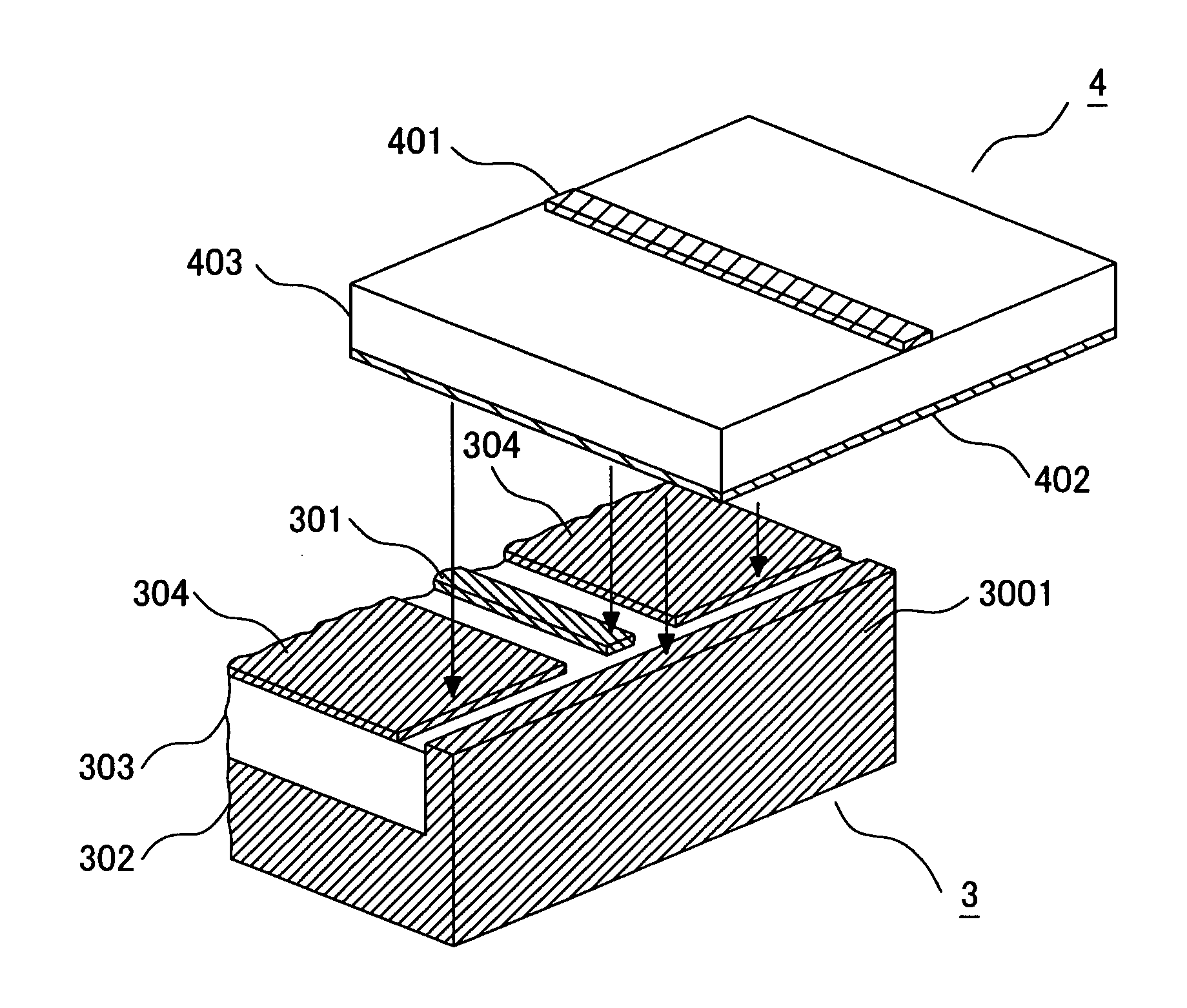
[0029] Referring to FIGS. 3A to 4E, the structure and method for connecting two transmission lines according to the invention will be described. One of transmission lines is a coplanar line with a ground and will be referred to as a component 3. The other of transmission lines is a microstrip line and will be referred to as a component 4. By connecting the signal wiring patterns of the two components 3 and 4 and by connecting the ground conductors of the two components 3 and 4, the two transmission lines are connected.
[0030] As shown in FIG. 3A, the lower component 3 includes a dielectric 303, a signal wiring pattern 301 and a ground conductor 304 both disposed on an upper surface of the dielectric 303, and a ground conductor 302 disposed on a lower surface of the dielectric 303.
[0031] In the first embodiment, the lower component 3 further includes a conductor 3001 disposed at an end surface thereof. The conductor 3001 is disposed perpendicular to the signal wiring pattern 301, suc...
second embodiment
[0052] Now referring to FIGS. 6A to 7E, the structure and method for connecting two transmission lines according to the invention will be described. One of transmission lines is a coplanar line with a ground and will be referred to as a component 5. The other of transmission lines is a microstrip line and will be referred to as a component 6. By connecting the signal wiring patterns of the two components 5 and 6 and by connecting the ground conductors of the two components 5 and 6, the two transmission lines are connected.
[0053] As shown in FIG. 6A, the lower component 5 includes a dielectric 503, a signal wiring pattern 501 and a ground conductor 504 both disposed at an upper surface of the dielectric 503, and a ground conductor 502 disposed on a lower surface of the dielectric 503.
[0054] In the second embodiment, the component 5 further includes a conductor 5001 disposed at an end surface thereof. The conductor 5001 is disposed perpendicular to the signal wiring pattern 501, such...
third embodiment
[0063] Now referring to FIGS. 8A through 9E, the structure and method for connecting two transmission lines according to the invention will be described. One of transmission lines is a microstrip line and will be referred to as a component 7. The other of transmission lines is a coplanar line with a ground and will be referred to as a component 8. By connecting the signal wiring patterns of the two components 7 and 8 and by connecting the ground conductors of the two components 7 and 8, the two transmission lines are connected.
[0064] As shown in FIG. 8A, the lower component 7 includes a dielectric 703, a signal wiring pattern 701 disposed on an upper surface of the dielectric 703, and a ground conductor 702 disposed on a lower surface of the dielectric 703.
[0065] In the third embodiment, the lower component 7 further includes a conductor 7001 disposed on an end surface thereof. The conductor 7001 is disposed perpendicular to the signal wiring pattern 701, such that it covers an end...
PUM
 Abstract
Description
Claims
Application Information