

Semiconductor memory device and method for initializing the same
- Summary
- Abstract
- Description
- Claims
- Application Information
AI Technical Summary
Benefits of technology
Problems solved by technology
Method used
Image

Examples
Embodiment Construction
[0046] An embodiment of the present invention will be described with reference to the drawings.
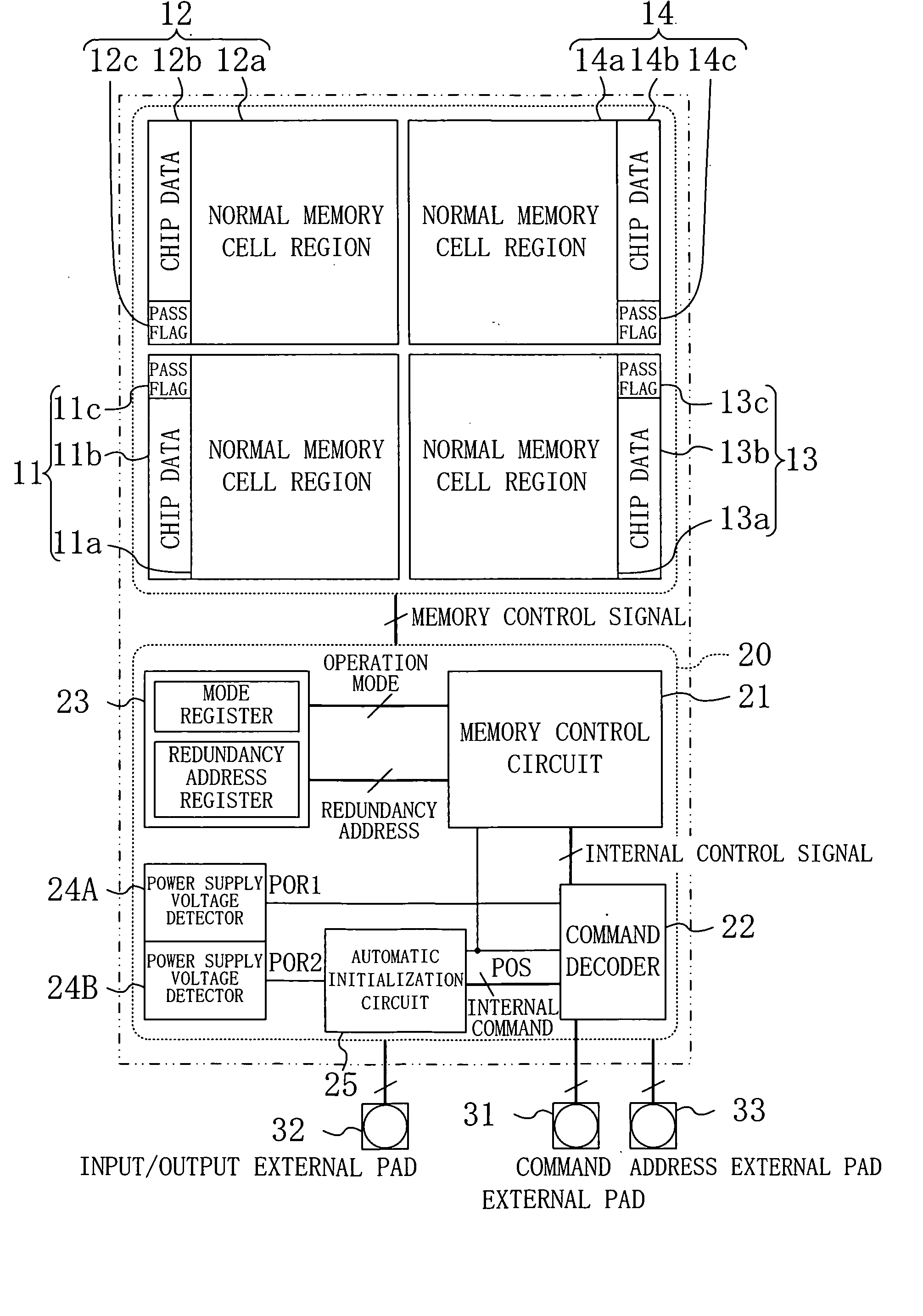
[0047]FIG. 1 shows a circuit configuration of a semiconductor memory device according to an embodiment of the present invention, which is a ferroelectric memory (FeRAM) with a capacitor including a capacitive film made of a ferroelectric.
[0048] As shown in FIG. 1, the semiconductor memory device of the embodiment includes a first memory cell block 11, a second memory cell block 12, a third memory cell block 13 and a fourth memory cell block 14, which are arranged in columns and rows and each of which is made up of a plurality of nonvolatile memory cells.
[0049] The first through fourth memory cell blocks 11 through 14 respectively include: first through fourth normal memory cell regions 11a through 14a storing user data; and first through fourth chip-data storing regions 11b through 14b including, for example, operation modes of respective memory cell blocks, addresses for redundancy rep...
PUM
 Abstract
Description
Claims
Application Information