Semiconductor Light Emitting Diode Chip

a technology of light-emitting diodes and semiconductors, applied in the direction of semiconductor devices, basic electric elements, electrical appliances, etc., can solve the problems of reducing the reliability of the chip, the area of the light-emitting compound is increased, and the nitride semiconductor used to generate the epitaxial layer is not a perfect crystal, etc., to achieve the effect of increasing the area of the light-emitting compound, increasing the adhesion of the pad on the surfa

Active Publication Date: 2016-08-25
YANGZHOU ZHONGKE SEMICON LIGHTING
View PDF59 Cites 3 Cited by
  • Summary
  • Abstract
  • Description
  • Claims
  • Application Information

AI Technical Summary

Benefits of technology

[0012]The beneficial effects of the present invention lie in that, corresponding graphical current extension layers are respectively disposed below an N pad and a P pad, and in all light emitting compound areas, there is electronic compound light emitting. Compared with the prior art, an area of a light emitting compound area is increased, which can effectively improve current distribution and light emitting brightness of a chip. In addition, graphical current extension can effectively increase an adhesion of a pad on a surface and improve the reliability of a chip.
[0013]To improve adhesion of a pad on a surface, on the basis of not affecting compound light emitting of a carrier of a semiconductor layer below a pad, according to the present invention, the graphical current extension layer is a current extension layer whose surface is of a net-dotted circular hole, and the diameter of the circular hole is less than 10 um.
[0014]In addition, a narrow side of the rectangular substrate is less than 300 um, which more benefits overflowing of a compounded photon of the pad below the semiconductor layer from a side wall.

Problems solved by technology

Large power means a large-size chip.
In addition, a Nitride semiconductor used to generate an epitaxial layer is not a perfect crystal.
Therefore, a chip having a larger size is easily affected by the defect density, which results in that the reliability of a chip is lowered, and a passing rate is lower relative to the small-size chip.
However, because the medium and small-sized chips have less light emitting areas, the medium and small-sized chips also greatly affect use of the small-sized chips for higher brightness.
In addition, an existing pad is generated on a flat and smooth plane and has bad adhesion, which results in that a chip pulls off a pad and is sealed off after suffering the hot-cold alternative temperature within an encapsulation body.

Method used


Image

  • Semiconductor Light Emitting Diode Chip
  • Semiconductor Light Emitting Diode Chip

Examples


Embodiment Construction

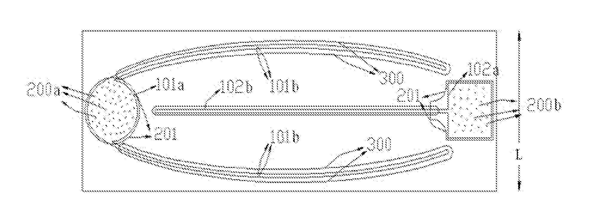
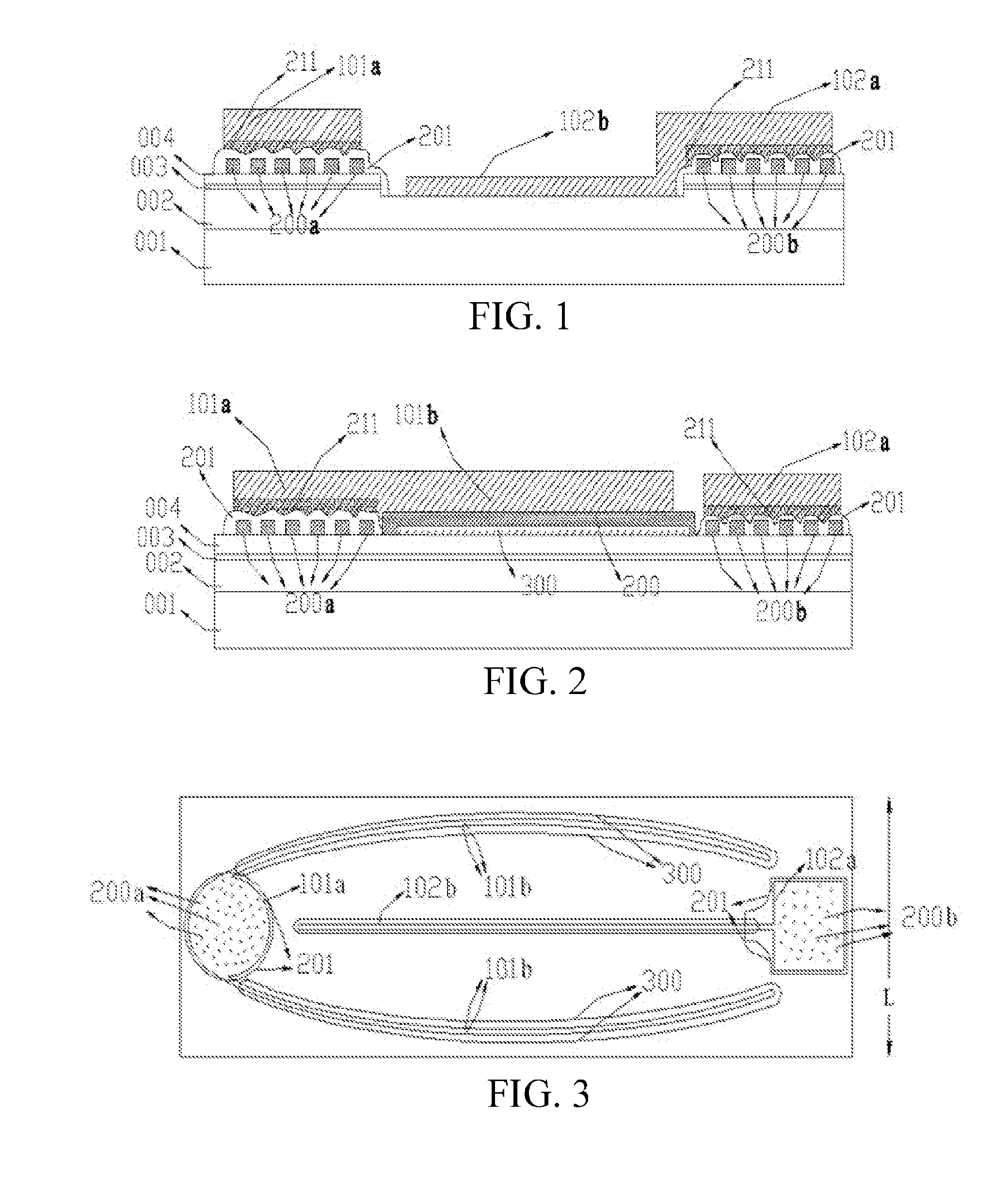
[0020]As shown in FIGS. 1, 2, and 3: An N-type semiconductor layer 002, a light emitting compound layer 003, and a P-type semiconductor layer 004, and an N-type semiconductor layer 002 that is exposed in the middle of the P-type semiconductor layer 004 after being etched are sequentially disposed on a rectangular substrate 001 having a narrow side L (which is as shown in FIG. 3) less than 300 um. P-type semiconductor layers 004 on two sides of the rectangular substrate 001 are respectively provided with a P pad 101a and an N pad 102a.

[0021]P-type semiconductor layers 004 corresponding to the P pad 101a and the N pad 102a are respectively provided with graphical current extension layers 200a and 200b, and the graphical current extension layers 200a and 200b are separately provided with an electrical-insulating layer 201.

[0022]The back of the P pad 101a and the back of the N pad 102a are separately provided with a reflector 211.

[0023]The P pad 101a is separately electrically connecte...


PUM


Abstract

A semiconductor light emitting diode chip relates to the field of production technologies of a light emitting diode. In the present invention, corresponding graphical current extension layers are respectively disposed below an N pad and a P pad, and in all light emitting compound areas, there is electronic compound light emitting. Compared with the prior art, an area of a light emitting compound area is increased, which can effectively improve current distribution and light emitting brightness of a chip. In addition, graphical current extension can effectively increase an adhesion of a pad on a surface and improve the reliability of a chip.

Description

BACKGROUND[0001]1. Technical Field[0002]The present invention relates to the field of production technologies of a light emitting diode, and in particular, to production technologies of a light emitting diode chip.[0003]2. Related Art[0004]With the advancement of epitaxial technologies, brightness of a semiconductor light emitting diode is improved year by year. According to power, a chip may be divided into a large-power chip, a medium-power chip, and a small-power chip. Large power means a large-size chip. However, 5 years before, large-size and large-power brightness now has been replaced with the medium-size chip, which has lower costs. Accordingly, the medium-power chip having a medium size in the past may be replaced with an existing small-size chip. In addition, a Nitride semiconductor used to generate an epitaxial layer is not a perfect crystal. In a generation process, because generation conditions between layers are different, crystal mismatch causes defects, where the def...

Claims


Application Information

Patent Timeline
Patent Type & Authority Applications(United States)
IPC IPC(8): H01L33/62H01L33/00H01L33/60
CPCH01L33/14H01L33/60H01L33/0016H01L33/62H01L33/38H01L33/405H01L33/44
Inventor JIN, YUZHEFENG, YAPINGZHANG, YILI, JIAJIALI, ZHICONGSUN, YIJUNWANG, GUOHONG
Owner YANGZHOU ZHONGKE SEMICON LIGHTING
Why Eureka
Try Eureka