Electrostatic chuck

a technology of electrostatic chuck and chuck body, which is applied in the direction of metal-working machine components, emergency protective circuit arrangements, manufacturing tools, etc., can solve the problems of difficult to allow thermally conductive gas, inability to achieve rapid control of wafer temperature, and inability to control the temperature of wafers. achieve the effect of improving plasma resistance and abrasion resistance and stable temperature controllability of substrates

Active Publication Date: 2005-09-22
TOKYO ELECTRON LTD
View PDF14 Cites 34 Cited by
  • Summary
  • Abstract
  • Description
  • Claims
  • Application Information

AI Technical Summary

Benefits of technology

[0009] The present invention has been conceived to solve the conventional problems described above. It is, therefore, an object of the present invention to provide an electrostatic chuck which is capable of improving plasma resistance and abrasion resistance thereof, and controlling the in-surface temperature of a substrate to be at a desired level or in a desired temperature distribution uniformly and rapidly, while preventing the substrate from springing up due to residual electric charges.
[0033] Preferably, each of the first and the second protrusion portions has a columnar shape with a same diameter not greater than 0.5 mm. In accordance with the present invention, there is provided an electrostatic chuck capable of improving plasma resistance and abrasion resistance, uniformly controlling the in-surface temperature over the entire surface of the substrate, and making the temperature controllability of the substrate stable.

Problems solved by technology

However, in case of an electrostatic chuck obtained by ceramic spraying, its wafer adsorption surface is weak, so that, for example, particles generated from the material of the wafer adsorption surface are likely to stick to a bottom surface of the wafer W, causing cross-contamination during a cleaning operation of the wafer W. Furthermore, the surface of the electrostatic chuck 1 may be roughened gradually as the adsorption and the separation process of the wafer W are repeated, and such a change in the surface state of the electrostatic chuck 1 makes it impossible to control the temperature of the wafer as in the initial stage.
However, the dots of the electrostatic chuck are of a low height of 5 μm or less, so that it is difficult to allow a thermally conductive gas to be uniformly distributed over the entire surface of the wafer W even though the thermally conductive gas is supplied into the gap between the electrostatic chuck and the wafer W. As a consequence, a rapid control of the wafer temperature cannot be realized.
Moreover, though groove portions are radially provided on the surface of the electrostatic chuck in order to distribute the thermally conductive gas over the entire surface of the wafer W, there frequently occurs a difference in heat transfer between the groove portions and the other portions, making it difficult to uniformly control the in-surface temperature of the wafer.
Furthermore, since the contact area of the dots and the wafer W amounts to about 20%, which is great, a desired temperature or a desired temperature distribution cannot be obtained by using the thermally conductive gas.
Still further, it is not sure that this electrostatic chuck has a plasma resistance.

Method used


Image

  • Electrostatic chuck
  • Electrostatic chuck
  • Electrostatic chuck

Examples


Embodiment Construction

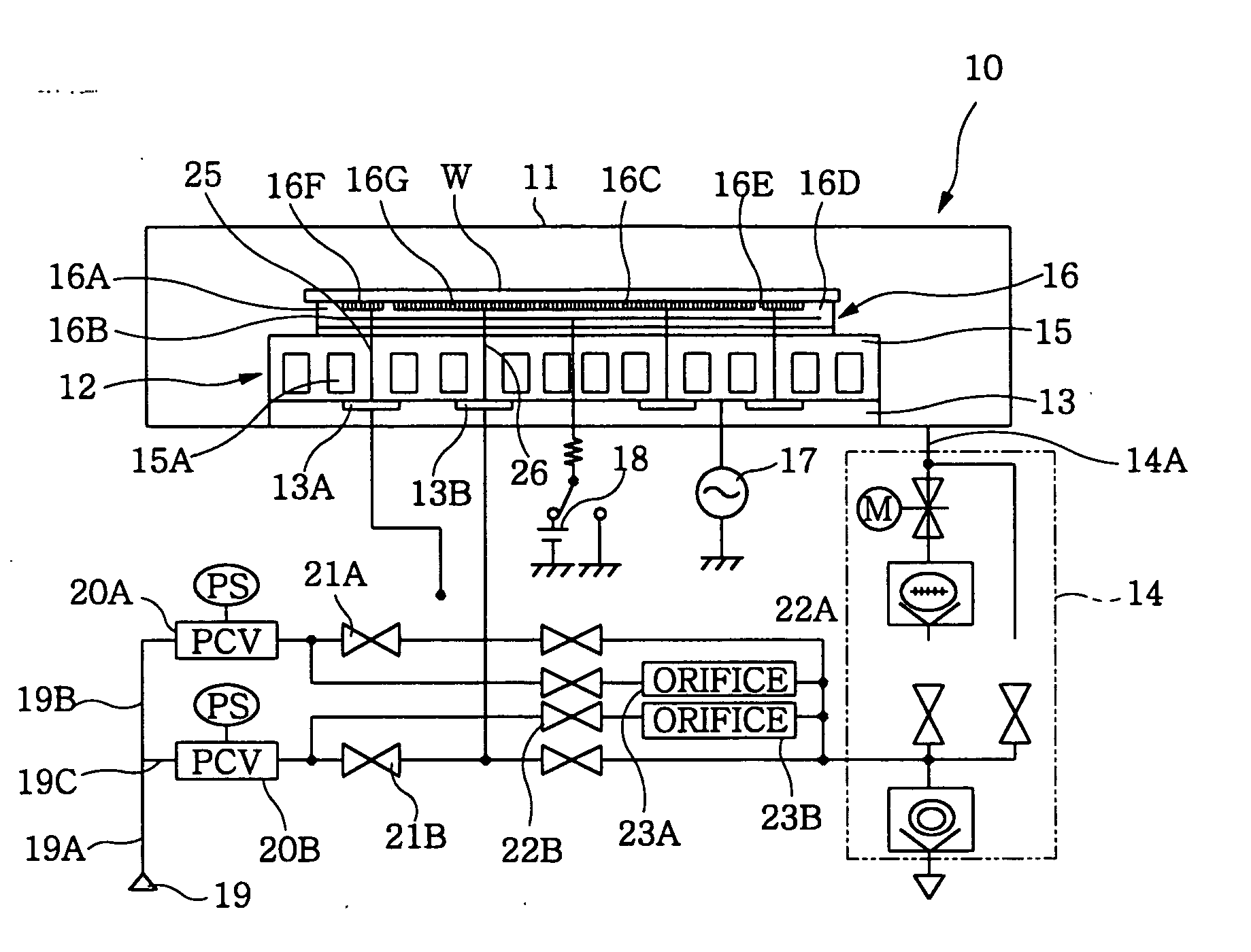
[0046] An electrostatic chuck in accordance with the present invention was used in, for example, a plasma processing apparatus, and desirable results could be obtained. Hereinafter, the electrostatic chuck employed in the plasma processing apparatus will be explained as an example.

[0047] The present invention will be described based on a preferred embodiment illustrated in FIGS. 1 to 11.

[0048] As shown in FIG. 1, for example, a plasma processing apparatus 10 in accordance with the present invention includes a chamber 11 capable of being maintained at a high vacuum level; a mounting body 12 disposed in the chamber 11 to mount thereon a substrate (for example, wafer) W; and an insulator 13 for electrically insulating the mounting body 12 from the chamber 11. Such a plasma processing apparatus 10 is configured to perform a preset plasma processing on the wafer W within the chamber 11 which is maintained at a predetermined vacuum level by a vacuum exhaust system 14 connected to the ch...


PUM

PropertyMeasurementUnit
Raaaaaaaaaaa
surface roughnessaaaaaaaaaa
diameteraaaaaaaaaa

Abstract

An electrostatic chuck for attracting and holding a substrate by using an electrostatic force includes a plurality of protrusion portions to be brought into contact with the substrate. The protrusion portions are formed of a ceramic dielectric including grains each having a specified particle diameter, and contact surfaces of the protrusion portions with the substrate are formed to have a surface roughness depending on the particle diameter.

Description

FIELD OF THE INVENTION [0001] The present invention relates to an electrostatic chuck for attracting and holding a substrate by employing an electrostatic force; and, more particularly, to an electrostatic chuck capable of improving abrasion resistance thereof and controlling the in-surface temperature of the substrate to be at a desired level during a processing of a substrate. BACKGROUND OF THE INVENTION [0002] As shown in FIG. 12, for example, a conventional electrostatic chuck 1 is employed as a part of a mounting body of a plasma processing apparatus in case of performing a plasma processing on a substrate (for example, wafer) W. Specifically, the electrostatic chuck 1 is used to attract and hold the wafer W on a top surface of the mounting body 2 by using an electrostatic force. Further, a focus ring 3 is disposed around a mounting surface of the mounting body 2 to surround the wafer W placed on the electrostatic chuck 1. [0003] Moreover, a high frequency power supply 4 is con...

Claims


Application Information

Patent Timeline
Patent Type & Authority Applications(United States)
IPC IPC(8): B23Q3/15H01L21/68H01L21/00H01L21/683H02H1/00
CPCH01L21/6831H01L21/67109H01L21/68
Inventor NISHIMOTO, SHINYANAKAYAMA, HIROYUKIKIMURA, HIDETOSHI
Owner TOKYO ELECTRON LTD
Why Eureka
Try Eureka