Solid-state imaging device, and method of driving solid-state imaging device

a solid-state imaging and imaging device technology, applied in the direction of radiation controlled devices, instruments, optical radiation measurement, etc., can solve the problems of lowering the resolution in at least one longitudinal and lateral direction, and it is difficult in general to widen the dynamic range, so as to achieve the effect of expanding the dynamic range without lowering the resolution

Inactive Publication Date: 2005-09-29
FUJIFILM CORP
View PDF5 Cites 18 Cited by
  • Summary
  • Abstract
  • Description
  • Claims
  • Application Information

AI Technical Summary

Benefits of technology

[0009] The invention has been conducted in view of the above-discussed circumstances. It is an object of the invention to provide a solid-state imaging device in which the dynamic range can be expanded without lowering the resolution.

Problems solved by technology

In a solid-state imaging device which is useful in a digital camera, charges corresponding to image signals are detected by photoelectric conversion elements, and hence it is difficult in general to widen the dynamic range.
However, the imaging device disclosed in JP-A-2001-238126 has a problem in that, when a picked-up image with an expanded dynamic range is to be obtained, the resolution in at least one of the longitudinal and lateral directions is lowered.

Method used


Image

  • Solid-state imaging device, and method of driving solid-state imaging device
  • Solid-state imaging device, and method of driving solid-state imaging device
  • Solid-state imaging device, and method of driving solid-state imaging device

Examples


first embodiment

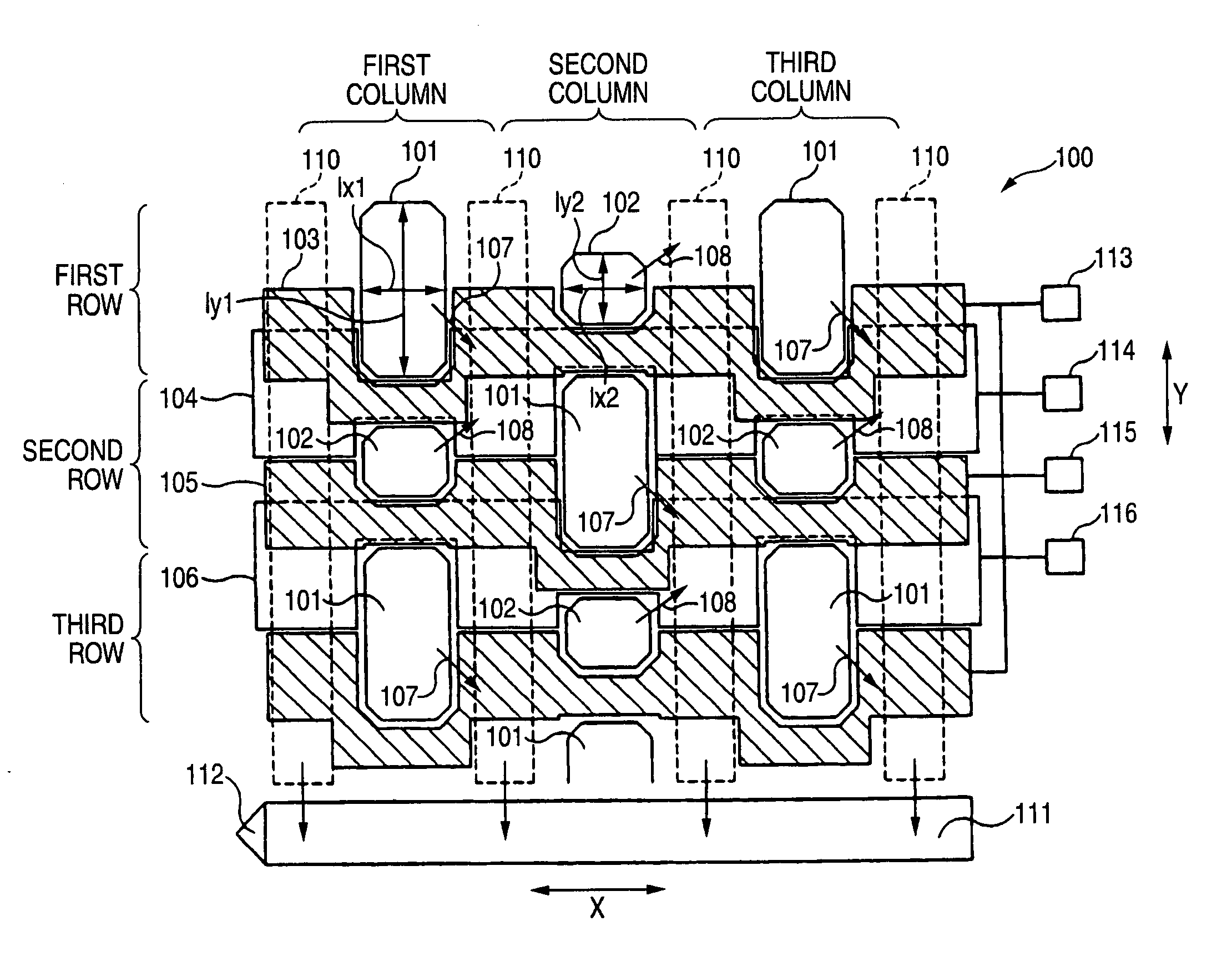
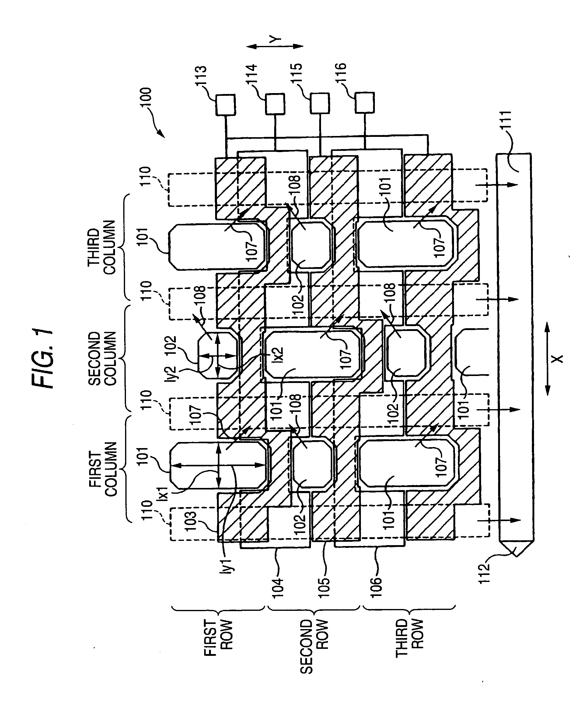
[0036]FIG. 1 is a view schematically showing the configuration of a solid-state imaging device 100 illustrating a first embodiment of the invention. FIG. 1 is a partial enlarged view of the solid-state imaging device 100.

[0037] The solid-state imaging device 100 includes: plural first photoelectric conversion elements 101 and second photoelectric conversion elements 102 (hereinafter, often referred to merely as photoelectric conversion elements) which are arranged in a square lattice on a surface of a semiconductor substrate in a row direction (the direction X in FIG. 1) and a column direction (the direction Y in FIG. 1) that is perpendicular to the row direction; vertical transfer portions 110 which are disposed to respectively correspond to plural photoelectric conversion element columns each configured by the photoelectric conversion elements that are arranged in the column direction, and which transfer charges from the photoelectric conversion elements in the column direction; ...

second embodiment

[0095]FIG. 13 is a view schematically showing the configuration of a solid-state imaging device illustrating a second embodiment of the invention. FIG. 13 is a partial enlarged view of the solid-state imaging device 300.

[0096] The solid-state imaging device 300 includes: plural first photoelectric conversion elements 301 and second photoelectric conversion elements 302 (hereinafter, often referred to merely as photoelectric conversion elements) which are arranged in a square lattice on a surface of a semiconductor substrate in a row direction (the direction X in FIG. 13) and a column direction (the direction Y in FIG. 13) that is perpendicular to the row direction; vertical transfer portions 310 which are disposed to respectively correspond to plural photoelectric conversion element columns each configured by the photoelectric conversion elements that are arranged in the column direction, and which transfer charges from the photoelectric conversion elements in the column direction;...


PUM


Abstract

A solid-state imaging device comprises: a semiconductor substrate; and a plurality of photoelectric conversion elements forming a square lattice pattern extending in a column direction and in a row direction substantially perpendicular to the row direction, on a surface of the semiconductor substrate, wherein said plurality of photoelectric conversion elements comprises: a plurality of first photoelectric conversion elements that conduct photoelectric conversion of a relatively higher sensitivity on an amount of incident light; and a plurality of second photoelectric conversion elements that conduct photoelectric conversion of a relatively lower sensitivity on the amount of incident light, wherein said plurality of first photoelectric conversion elements and said plurality of second photoelectric conversion elements are arranged in respective checkered patterns, and wherein said plurality of first photoelectric conversion elements are larger in size than said plurality of second photoelectric conversion elements.

Description

BACKGROUND OF THE INVENTION [0001] 1. Field of the Invention [0002] The present invention relates to a solid-state imaging device including plural photoelectric conversion elements which are arranged in a square lattice on a semiconductor substrate in a row direction and a column direction that is perpendicular to the row direction. [0003] 2. Description of the Related Art [0004] In a solid-state imaging device which is useful in a digital camera, charges corresponding to image signals are detected by photoelectric conversion elements, and hence it is difficult in general to widen the dynamic range. In order to obtain an image of a wide dynamic range, therefore, it has been proposed to use a solid-state imaging device having relatively higher-sensitive photoelectric conversion elements, and relatively lower-sensitive photoelectric conversion elements (see JP-A-2001-238126). [0005] In the imaging device disclosed in JP-A-2001-238126, rows of the high-sensitive photoelectric conversio...

Claims


Application Information

Patent Timeline
Patent Type & Authority Applications(United States)
IPC IPC(8): H04N5/335H01L27/148H04N5/341H04N5/347H04N5/355H04N5/357H04N5/369H04N5/372H04N5/376H04N9/04H04N9/07H04N101/00
CPCH04N9/045H04N23/84H04N25/134
Inventor ODA, KAZUYASAKAMOTO, TOMOHIRO
Owner FUJIFILM CORP
Why Eureka
Try Eureka