Flip-flop circuit and frequency division circuit using same

a flip-flop circuit and circuit technology, applied in the field of flip-flop circuits, can solve the problems of circuits insufficient for low-voltage operation and operation frequency drop, and achieve the effect of low-voltage operation

Inactive Publication Date: 2005-10-06
PANASONIC CORP
View PDF8 Cites 1 Cited by
  • Summary
  • Abstract
  • Description
  • Claims
  • Application Information

AI Technical Summary

Benefits of technology

[0020] In order to attain the above-described object the flip-flop circuit in accordance with the present invention has a three-stage configuration of transistors connected between the power source voltage and GND, this configuration being identical to the conventional configuration. In this configuration, using bipolar transistors for the upper-stage transistors of the three-stage structure enables the circuit to operate in a frequency range up to a high frequency, and using MOS transistors with a low threshold for the transistors of the medium and lower stages of the three-stage structure of the flip-flop circuit ensures low-voltage operation.

Problems solved by technology

However, because MOS transistors have a frequency characteristic worse that that of the bipolar transistors, the operation frequency decreases.
In the conventional flip-flop circuit 21 using bipolar transistors shown in FIG. 2, the minimum necessary power source voltage is high, making the circuit inadequate for low-voltage operation.

Method used


Image

  • Flip-flop circuit and frequency division circuit using same
  • Flip-flop circuit and frequency division circuit using same
  • Flip-flop circuit and frequency division circuit using same

Examples


Embodiment Construction

[0030] The preferred embodiments of the present invention will be described below with reference to FIG. 1.

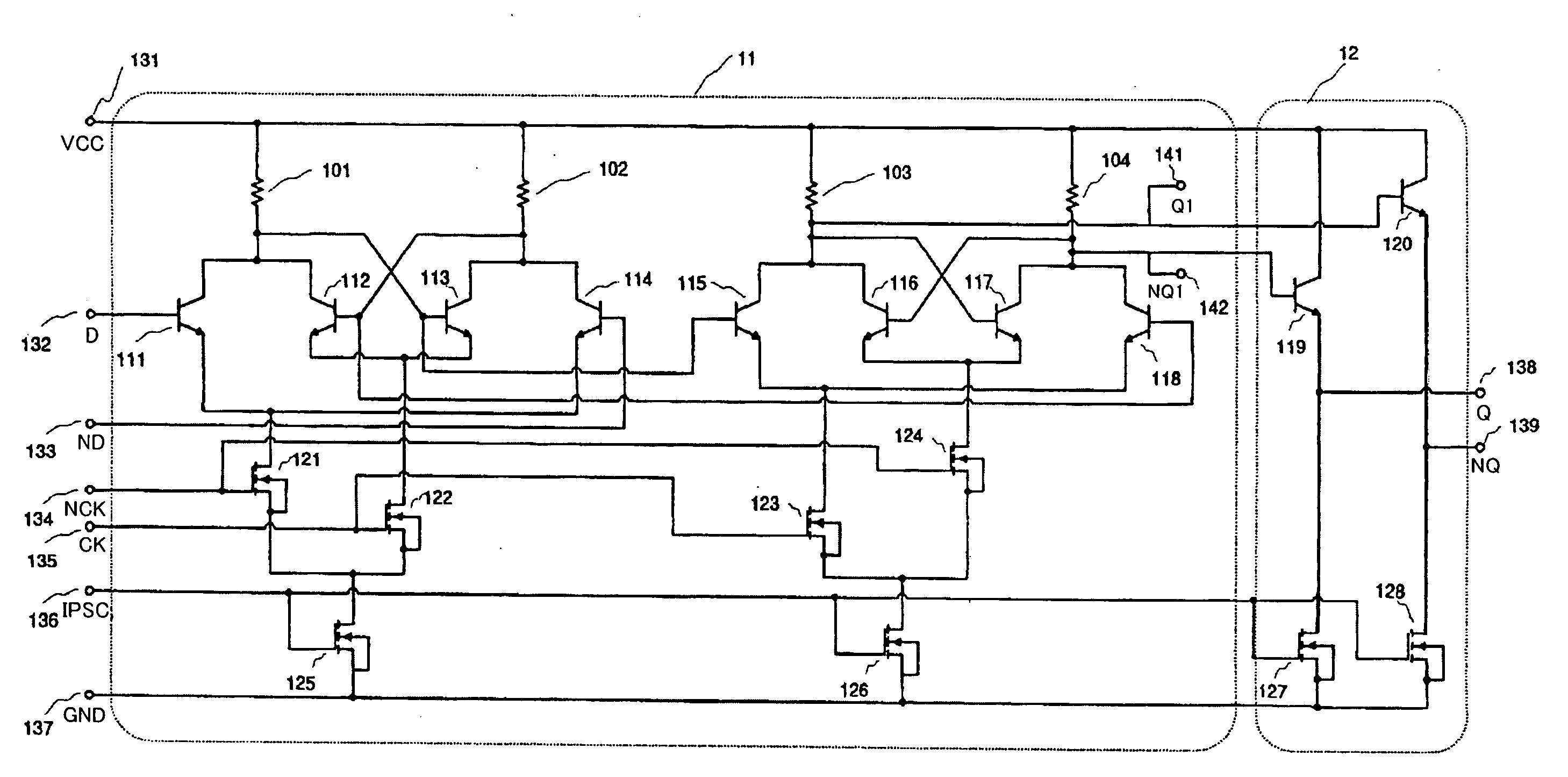
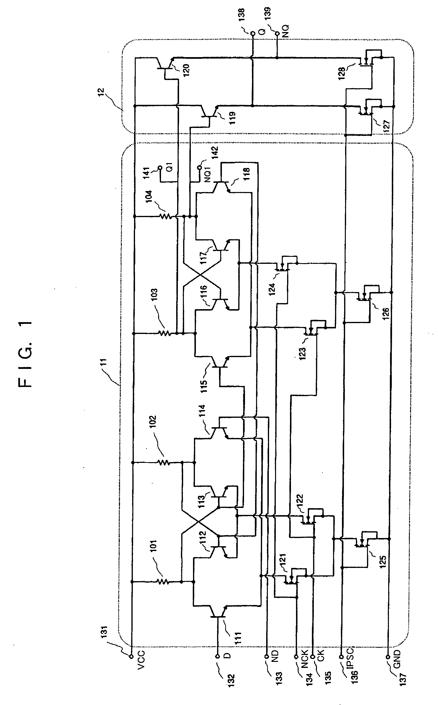
[0031]FIG. 1 is a structural drawing illustrating a frequency division circuit of the embodiment of the present invention, this circuit comprising a flip-flop circuit 11 and a buffer circuit 12. Referring to FIG. 1, the reference numerals 101-104 stand for load resistors, 111-120—bipolar transistors, 121-128—MOS transistors. The MOS transistors 121-128 comprise low-threshold MOS transistors.

[0032] The flip-flop circuit 11 is produced by connecting the load resistors 101-104, bipolar transistors 111-118, and MOS transistors 121-126 as shown in FIG. 1. The buffer circuit 12 is provided by connecting the bipolar transistors 119, 120 and MOS transistors 127, 128 as shown in FIG. 1.

[0033] The bipolar transistor 111 and bipolar transistor 114, bipolar transistor 112 and bipolar transistor 113, bipolar transistor 115 and bipolar transistor 118, bipolar transistor 116 and bipolar tr...


PUM


Abstract

An object of the present invention is to obtain a frequency division circuit including a flip-flop circuit capable of low-voltage and high-frequency operation. The frequency division circuit has bipolar transistors and MOS transistors. Thus, the circuit includes transistors that are connected to the transistor to which the clock input is input, that execute the differential operation after being input with data input signals, and that output signals of resistors, and also transistors that are similarly connected to the transistor to which Ck is input and that hold signals of resistors, transistors that are connected to the transistor to which Ck is input and that output signals of resistors, and transistors that are connected to the transistor to which NCk is input and that hold signals of resistors.

Description

BACKGROUND OF THE INVENTION [0001] 1. Field of the Invention [0002] The present invention relates to a frequency division circuit using a flip-flop circuit combining therein bipolar transistors and MOS transistors and a buffer circuit. [0003] 2. Description of the Related Art [0004]FIG. 2 shows a conventional frequency division circuit comprising a flip-flop circuit 21 using bipolar transistors and a buffer circuit 22. The reference numerals 211-228 stand for bipolar transistors, 231—a power source voltage terminal, 201-204—load resistors, 205-208—resistors determining the current of a constant current source. Pairs of transistor 211 and transistor 214, transistor 212 and transistor 213, transistor 215 and transistor 218, transistor 216 and transistor 217, transistor 221 and transistor 222, and transistor 223 and transistor 224 form respective differential pairs. A data signal D is inputted to the base of the bipolar transistor 211, and a data signal ND is inputted to the base of th...

Claims


Application Information

Patent Timeline
Patent Type & Authority Applications(United States)
IPC IPC(8): H03K3/2885H03K3/286H03K3/289H03K3/356H03K19/08
CPCH03K3/289H03K3/2885
Inventor OSAKO, SHINICHI
Owner PANASONIC CORP
Why Eureka
Try Eureka