Semiconductor memory device

A memory and semiconductor technology, used in semiconductor devices, static memory, digital memory information, etc., can solve problems such as large standby current, latch-up, and radiation soft error.

Active Publication Date: 2016-10-12
POWERCHIP SEMICON MFG CORP
View PDF9 Cites 0 Cited by
  • Summary
  • Abstract
  • Description
  • Claims
  • Application Information

AI Technical Summary

Problems solved by technology

[0029] (1) The size of the memory cell is relatively large, and the memory cost also increases
[00

Method used


Image

  • Semiconductor memory device
  • Semiconductor memory device
  • Semiconductor memory device

Examples


Embodiment 1

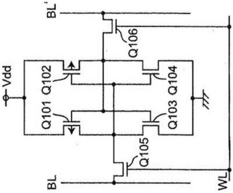
[0112] figure 2 is a circuit diagram illustrating a configuration example of a storage capacitor type SRAM related to Embodiment 1 of the present invention. image 3 is description figure 2 A longitudinal cross-sectional view of the construction of a part of a storage capacitor type SRAM.

[0113] see figure 2 , the storage capacitor type SRAM of Embodiment 1 includes 4 MOS transistors Q1T, Q2T, Q3, Q4 forming latches and 2 N-channel access transistors all located between bit lines BL, BL' and word line WL MOS transistors Q5, Q6. Here, MOS transistors Q1T, Q2T are TFT type P-channel MOS transistors and the other four MOS transistors Q3 to Q6 are embedded gate type N-channel body transistors (for example, refer to Patent Document 1). Among the semiconductor layer structures of MOS transistors, a current storage capacitor type SRAM is characterized in that an embedded gate is constituted by forming an embedded for accommodating a gate electrode and then forming a gate ele...

Embodiment 2

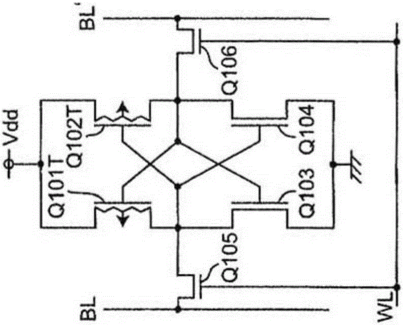
[0123] Figure 4 It is a circuit diagram illustrating a configuration example of a storage capacitor type SRAM related to Embodiment 2 of the present invention. Figure 5 is description Figure 4 A longitudinal cross-sectional view of a part of the construction of a storage capacitor type SRAM.

[0124] compare about Figure 4 The storage capacitor type SRAM in Example 2 with respect to figure 2 In the storage capacitor type SRAM of Embodiment 1, the differences are described below.

[0125] (1) TFT-type N-channel MOS transistors Q3T, Q4T are included to replace figure 2 The main body MOS transistors Q3, Q4.

[0126] (2) by having Figure 5 TFT MOS transistors Q1T, Q3T are formed by vertical integrated TFT MOS transistors Q1T, Q3T in the same gate region TG.

[0127] (3) by having Figure 5 TFT MOS transistors Q2T, Q4T are formed by vertical integrated TFT MOS transistors Q2T, Q4T in the same gate region TG.

[0128] exist Figure 5Among them, MOS transistors Q1T, ...

Embodiment 3

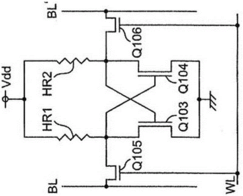
[0141] Image 6 It is a circuit diagram illustrating a configuration example of a storage capacitor type SRAM related to Embodiment 3 of the present invention. Figure 7 are instructions for Image 6 A longitudinal sectional view of the structure of the silicon-on-insulator (SOI) type access MOS transistors Q5L, Q6L in the storage capacitor type SRAM of .

[0142] compare about Image 6 The storage capacitor type SRAM in Example 3 with respect to figure 2 In the storage capacitor type SRAM of Embodiment 1, differences are described as follows.

[0143] (1) A body leakage MOS transistor Q5L having a back gate control terminal LT is included instead of the access MOS transistor Q5.

[0144] (2) A capacitor C3 is included instead of the MOS transistor Q3, wherein one end of the capacitor C3 is connected to the node P2 and the other end of the capacitor C3 is connected to the back gate control terminal LT of the leaky MOS transistor Q5L.

[0145] (3) A body leakage MOS trans...


PUM


Abstract

The semiconductor memory device of the invention includes 2 TFT MOS transistors, 2 bulk MOS transistors, a first and second access MOS transistors and a first and second capacitor. The TFT and bulk MOS transistors form a latch for retaining a data that is inverted between a first and second node. The first bulk access MOS transistor switches the first node to connect to a first bit line according to a voltage of a word line. The second bulk access MOS transistor, switches the second node to connect to a second bit line according to the voltage of the word line. The first capacitor is disposed between the first node and a power supply voltage. The second capacitor is disposed between the second node and the power supply voltage. The bulk MOS transistors and the access MOS transistors are formed by a recess gate type MOS transistor.

Description

technical field [0001] The present invention relates to semiconductor memory devices, and more particularly to volatile semiconductor memory devices, such as Static Random Access Memory (SRAM). [0002] cross of related applications [0003] Citing this application claims the priority of Japanese application No. 2015-064413 filed on March 26, 2015. The above patent application is hereby incorporated by reference in its entirety and constitutes a part of this specification. Background technique [0004] SRAM is a volatile semiconductor memory device, and can be defined as a volatile RAM that does not require activation of internal circuits for retaining data. Generally, a flip-flop acts as a component for holding data and is the basic structure of RAM. Due to the introduction of Dynamic Random Access Memory (Dynamic Random Access Memory; DRAM), which requires a new RAM in order to keep data, the modifier "static" is added for distinction. In addition to transistors, circu...

Claims


Application Information

Patent Timeline
IPC IPC(8): H01L27/11G11C11/41G11C11/412
CPCG11C11/41G11C11/412H10B10/00H10B10/12H01L27/0207H01L28/90G11C11/4125H10B10/125
Inventor 木原雄治
Owner POWERCHIP SEMICON MFG CORP
Why Eureka
Try Eureka