

Two bit/four bit SONOS flash memory cell
a sonos flash memory and sonos technology, applied in semiconductor devices, electrical devices, instruments, etc., can solve the problems of difficult to read bitb>1/b> from bitb>2/b>, difficult to scale the channel length of the nrom memory cell below 100 nm, etc., to prevent lateral charge migration and more controllable charge injection locations
- Summary
- Abstract
- Description
- Claims
- Application Information
AI Technical Summary
Benefits of technology
Problems solved by technology
Method used
Image

Examples
Embodiment Construction
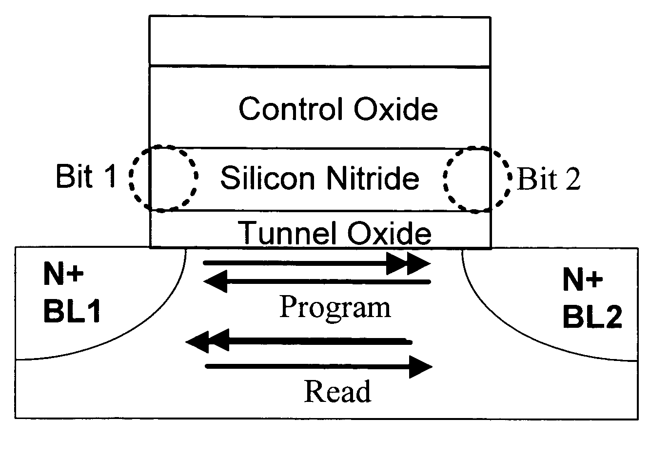
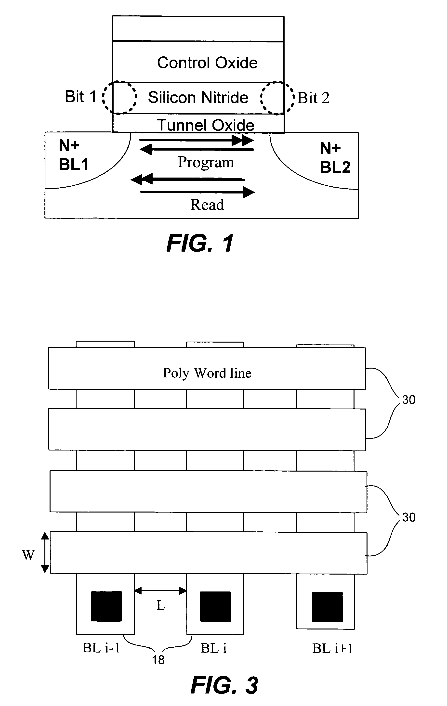
[0026] One Embodiment of the invention is a novel two-bit per cell SONOS flash memory that is scalable to sub 50 nm technology generation. The novel memory structure takes the advantage of both the NROM technology and a spacer technology, the nitride charge storage site at Bit1 and Bit2 are physically separated from each other by thermal oxide. Hence the lateral charge migration is eliminated and the charge injection location is more controllable by controlling the lateral dimension of the nitride charge storage site.
[0027] Buried bit line layout is utilized in the NROM memory, so the number of the bit line contacts along each bit line can be reduced to achieve small memory cell size. The process flow to fabricate our proposed memory structure is compatible with buried bit line layout, although other types of flash memory with nitride storage site formed by spacer technology are not compatible with buried bit line layout.
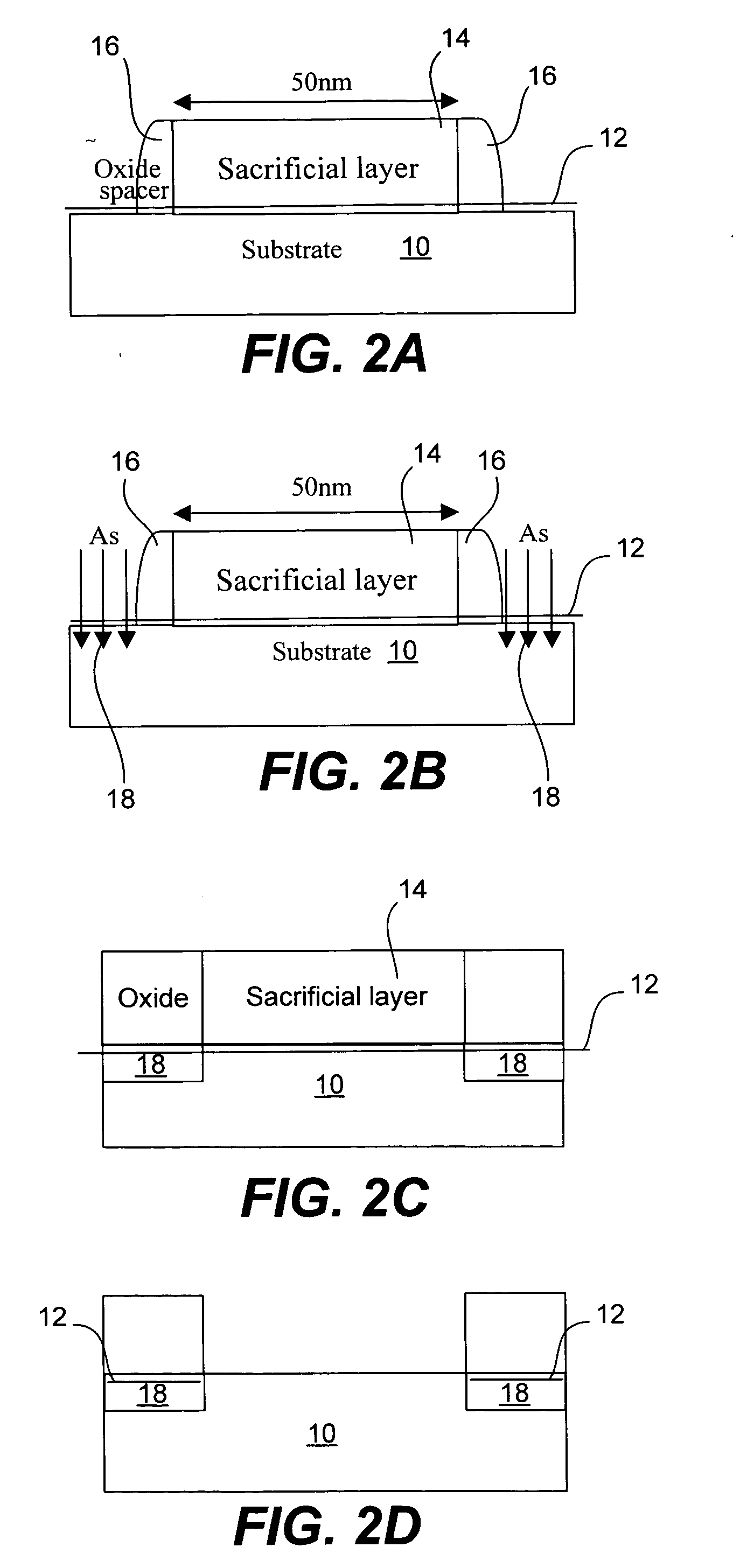
[0028] As shown in FIG. 2, a sacrificial layer 14 (for examp...
PUM
 Abstract
Description
Claims
Application Information