Semiconductor light emitting device on insulating substrate and its manufacture method

a technology of semiconductor devices and light emitting devices, which is applied in the direction of semiconductor devices, semiconductor/solid-state device details, electrical devices, etc., can solve problems such as current supply disturbance, light emission variations, and actualization of problems, and achieve the effect of efficient supply

Active Publication Date: 2005-11-17
STANLEY ELECTRIC CO LTD
View PDF6 Cites 84 Cited by
  • Summary
  • Abstract
  • Description
  • Claims
  • Application Information

AI Technical Summary

Benefits of technology

[0012] An object of this invention is to provide a semiconductor light emitting device having a nitride semiconductor light emission layer, capable of supplying current readily to a whole light emission region and efficiently providing a high light output, and its manufacture method.
[0013] Another object of this invention is to provide a semiconductor light emitting device having a nitride semiconductor light emission layer, capable of efficiently emitting light in a broad light emission region.
[0016] A plurality of mesa active regions surrounded by the recess regions are formed in the light emission area, one electrode is formed on the recess regions surrounding the mesa active regions and the other electrodes are formed on the mesa active regions. Accordingly, current can be supplied efficiently at a low resistance to any position in the light emission area.

Problems solved by technology

As the die size becomes large, some problems have been actualized, such as light emission variations, current supply disturbances and device exothermic.

Method used


Image

  • Semiconductor light emitting device on insulating substrate and its manufacture method
  • Semiconductor light emitting device on insulating substrate and its manufacture method
  • Semiconductor light emitting device on insulating substrate and its manufacture method

Examples


first embodiment

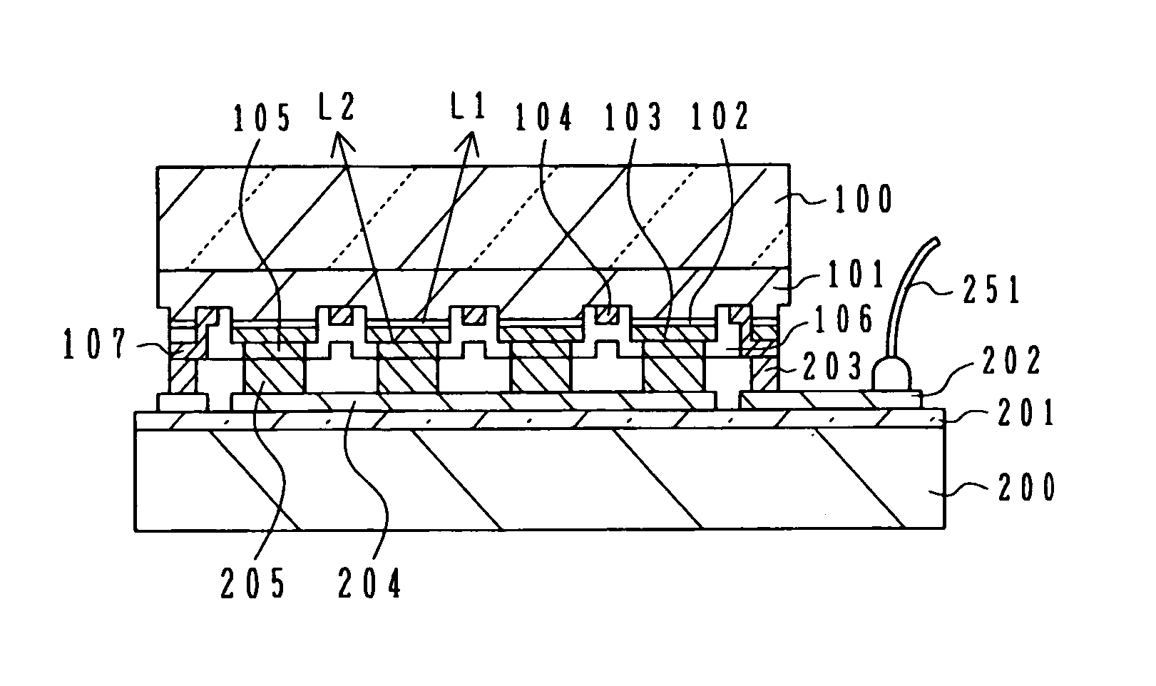
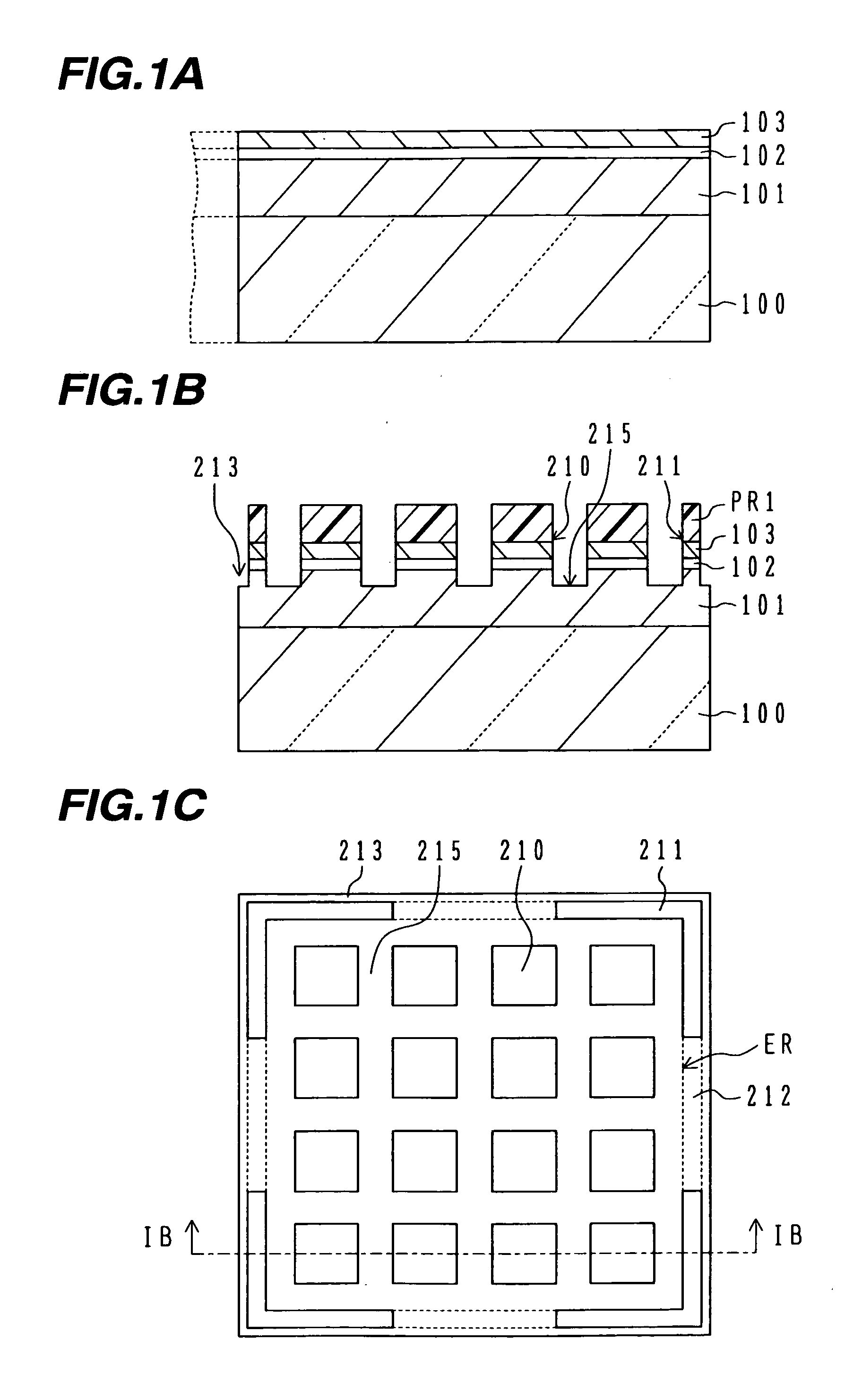
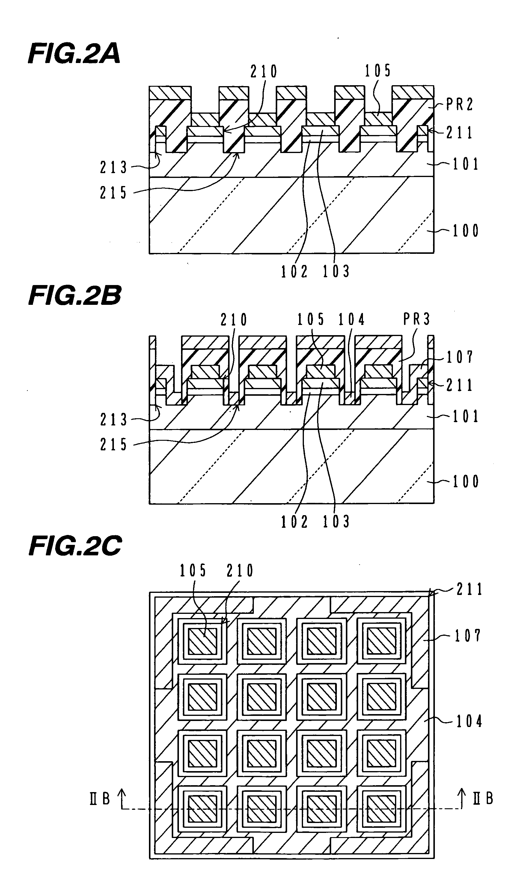
[0032]FIGS. 1A to 1C, FIG. 2A to 2C, FIG. 3, FIGS. 4A and 4B and FIGS. 5A to 5C are cross sectional views and plan views illustrating a method for manufacture a semiconductor light emitting device according to the invention. FIGS. 1A to 1C, FIG. 2A to 2C and FIG. 3 are cross sectional views and plan views of a semiconductor light emitting device substrate, FIGS. 4A and 4B are a cross sectional view and a plan view of a support substrate, and FIGS. 5A to 5C are cross sectional views and a plan view of the semiconductor light emitting device having a semiconductor light emitting device substrate bonded to the support substrate.

[0033] As shown in FIG. 1A, on the surface of a sapphire substrate 100, a GaN series nitride semiconductor layers 101, 102 and 103 are epitaxially grown. Epitaxial growth can be performed by metal organic vapor phase epitaxial (MOVPE) growth, molecular beam epitaxial (MBE) growth or the like.

[0034] If necessary, a buffer layer of GaN series nitride semiconducto...

third embodiment

[0108]FIGS. 8A to 8E show the In this embodiment, a hardly wettable protection film is formed on both the light emitting device substrate and support substrate, the number of mesa active regions is set to 2, and the shape of the mesa active region and mesa electrode pull-up region is rectangular.

[0109]FIGS. 8A and 8B are a cross sectional view and a plan view of the light emitting device substrate. Similar to the above-described embodiments, stacked on a transparent single crystal substrate 500 are an n-type layer 501, a light emission layer 502 and a p-type layer 503 respectively made of GaN series nitride semiconductor. A region other than mesa regions are etched by reactive ion etching to leave mesa active regions 510 and mesa electrode pull-up regions 511.

[0110] By using a photoresist mask, electron beam vacuum deposition and lift-off, on the n-type layer 501 exposed in the recess area, an n-side ohmic electrode 504 is formed which continuously extends to the upper surface of ...


PUM


Abstract

A semiconductor LED device includes: a transparent substrate stacked on which are an n-type nitride semiconductor layer, a nitride semiconductor light emission layer and a p-type nitride semiconductor layer; recess regions cutting the p-type layer and light emission layer and exposing the n-type layer, defining a plurality of mesa active regions and mesa electrode pull-up regions; an n-side electrode formed on the n-type layer in the recess surrounding the mesa active regions and extending onto the mesa electrode pull-up regions; a p-side electrode formed on the p-type layer of each of the mesa active regions; and a support substrate including n-side connection members connected to and facing the n-type electrodes and p-side connection members connected to and facing the p-side electrodes.

Description

CROSS REFERENCE TO RELATED APPLICATION [0001] This application is based on and claims priority of Japanese Patent Application No. 2004-141380 filed on May 11, 2004, the entire contents of which are incorporated herein by reference. BACKGROUND OF THE INVENTION [0002] A) Field of the Invention [0003] The present invention relates to a semiconductor light emitting device and its manufacture method, and more particularly to a semiconductor light emitting device having a semiconductor light emission structure formed on a transparent single crystal substrate such as sapphire and its manufacture method. [0004] B) Description of the Related Art [0005] Semiconductor light emitting devices for blue light emission are widely known which utilize nitride semiconductor (called GaN series (compound) semiconductor) such as GaN, GaAlN, InGaN and InAlGaN. If a light emitting diode (LED) for blue light emission is covered with a wavelength conversion layer which contains fluorescent material, white li...

Claims


Application Information

Patent Timeline
Patent Type & Authority Applications(United States)
IPC IPC(8): H01L29/06H01L33/06H01L33/14H01L33/20H01L33/32H01L33/34H01L33/38H01L33/40
CPCH01L33/08H01L2224/13H01L33/38H01L33/20H01L2224/05001H01L2224/16227H01L2224/0603
Inventor HORIO, NAOCHIKATSUCHIYA, MASAHIKOKATO, MUNEHIRO
Owner STANLEY ELECTRIC CO LTD
Why Eureka
Try Eureka