

Memory device having an electron trapping layer in a high-K dielectric gate stack
- Summary
- Abstract
- Description
- Claims
- Application Information
AI Technical Summary
Benefits of technology
Problems solved by technology
Method used
Image

Examples
Example
[0018] It is to be understood that in the drawings like reference numerals designate like structural elements. Also, it is understood that the depictions in the drawings are not necessarily to scale.
DETAILED DESCRIPTION OF THE DRAWINGS
[0019] The present invention has been particularly shown and described with respect to certain embodiments and specific features thereof. The embodiments set forth hereinbelow are to be taken as illustrative rather than limiting. It should be readily apparent to those of ordinary skill in the art that various changes and modifications in form and detail may be made without departing from the spirit and scope of the invention.
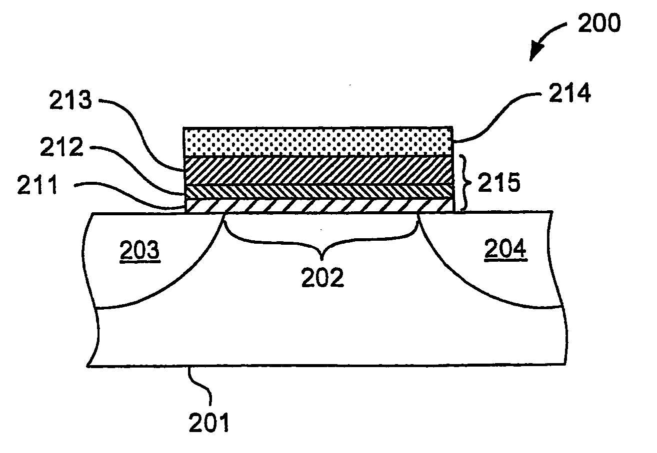
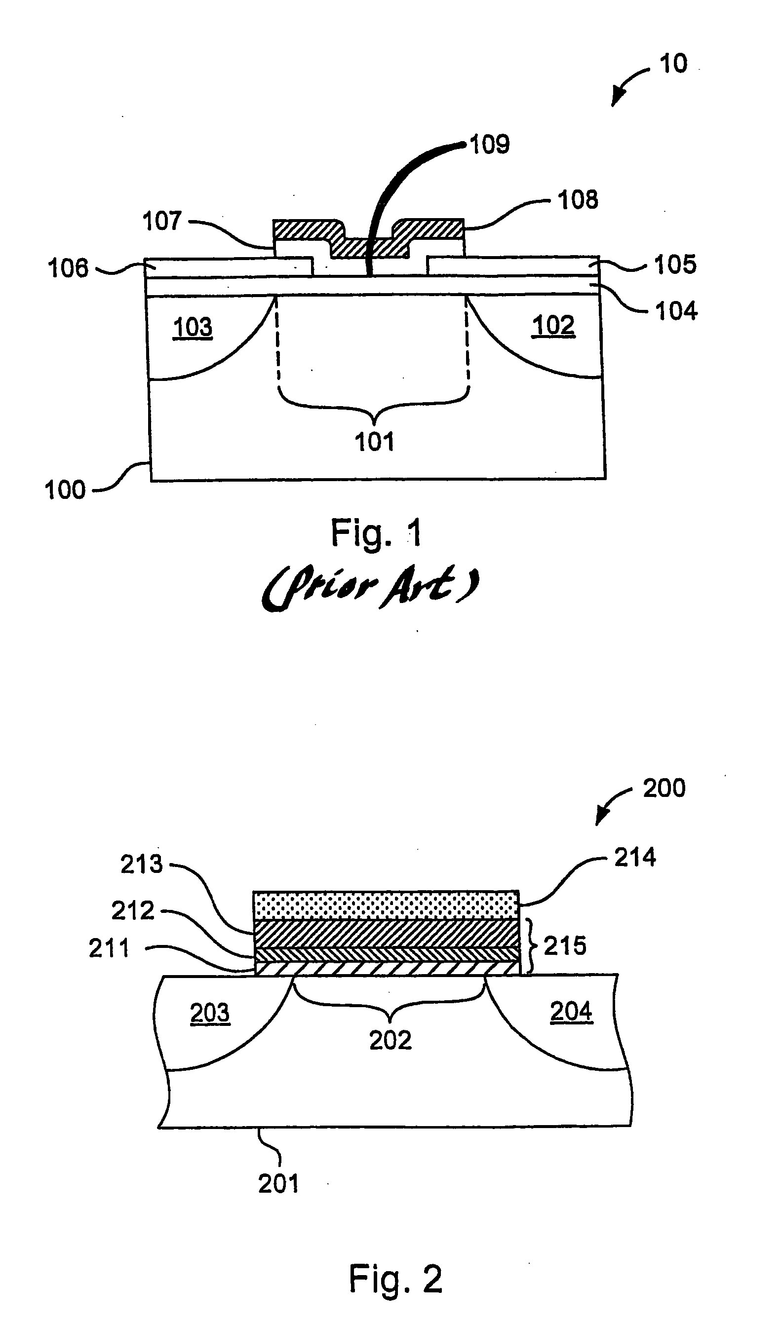
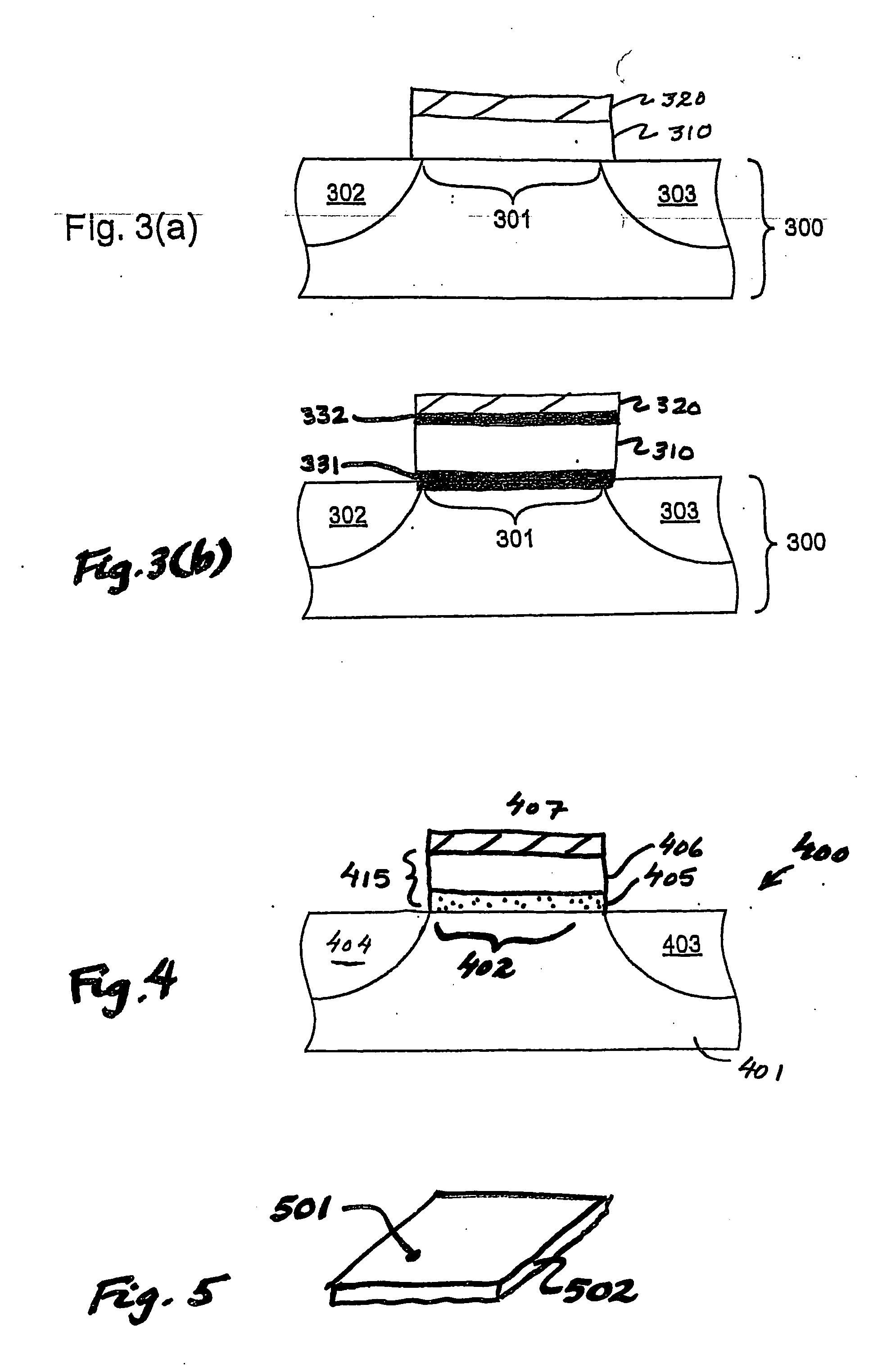
[0020] Embodiments of the present invention are directed to memory structures having an electron trapping layer and the methods of forming such memory structures. In such structures a high-K electron trapping layer is formed as part of (or in some embodiments the entirety of) a dielectric gate stack formed on a channel portion o...
PUM
 Abstract
Description
Claims
Application Information