Non-volatile semiconductor storage device

a storage device and non-volatile technology, applied in the direction of semiconductor devices, electrical appliances, transistors, etc., can solve the problems of increasing the difficulty of continuously advancing the cell size of memory cells based on a reduction in the minimum feature siz

Inactive Publication Date: 2008-06-05
KK TOSHIBA
View PDF2 Cites 172 Cited by
  • Summary
  • Abstract
  • Description
  • Claims
  • Application Information

AI Technical Summary

Benefits of technology

[0008]According to one aspect of the present invention, there is provided a non-volatile semiconductor storage device comprising: a first non-volatile memory cell provided on a first insulator above a substrate; and a second non-volatile memory cell provided on a second insulator above the first non-volatile memory cell, wherein the first non-volatile memory cell includes: a first semiconductor layer including an n-type region and a p-type region; and a first gate stack which is provided above the first semiconductor layer and includes a first

Problems solved by technology

In a non-volatile semiconductor storage device, further continuously advancing a cell size of a memory cell based on a reduction in

Method used


Image

  • Non-volatile semiconductor storage device
  • Non-volatile semiconductor storage device
  • Non-volatile semiconductor storage device

Examples


first embodiment

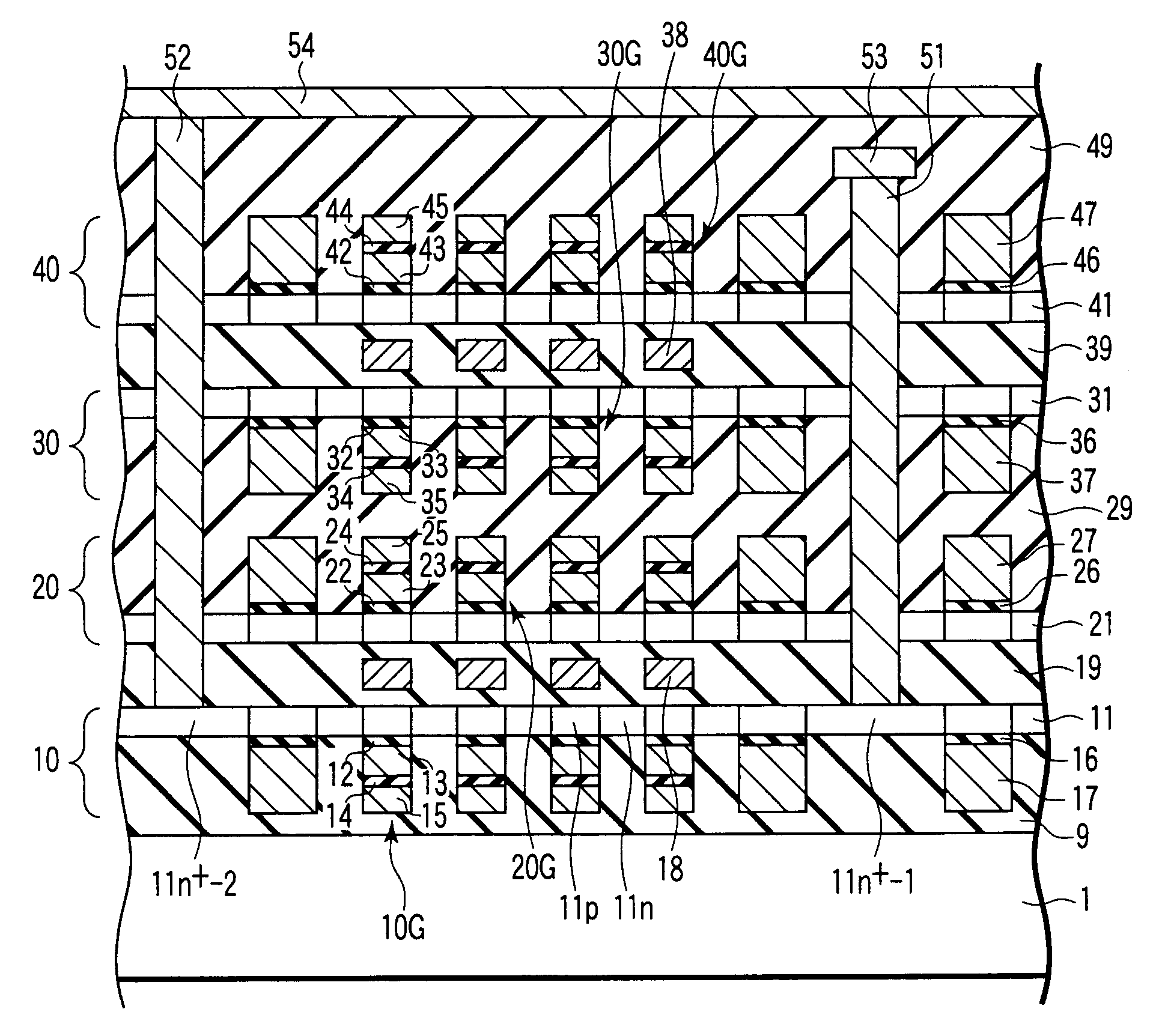
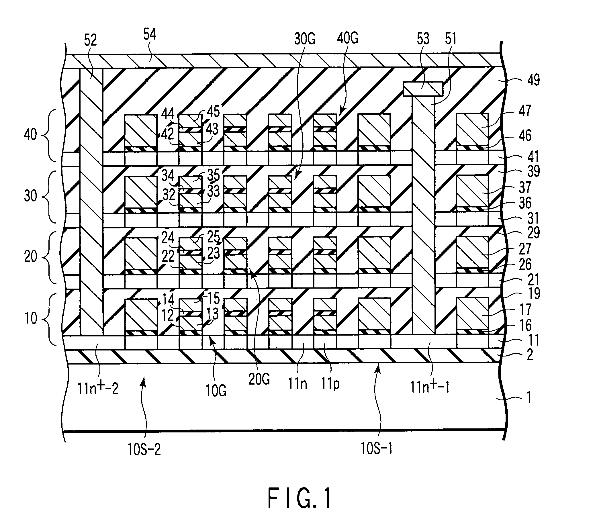
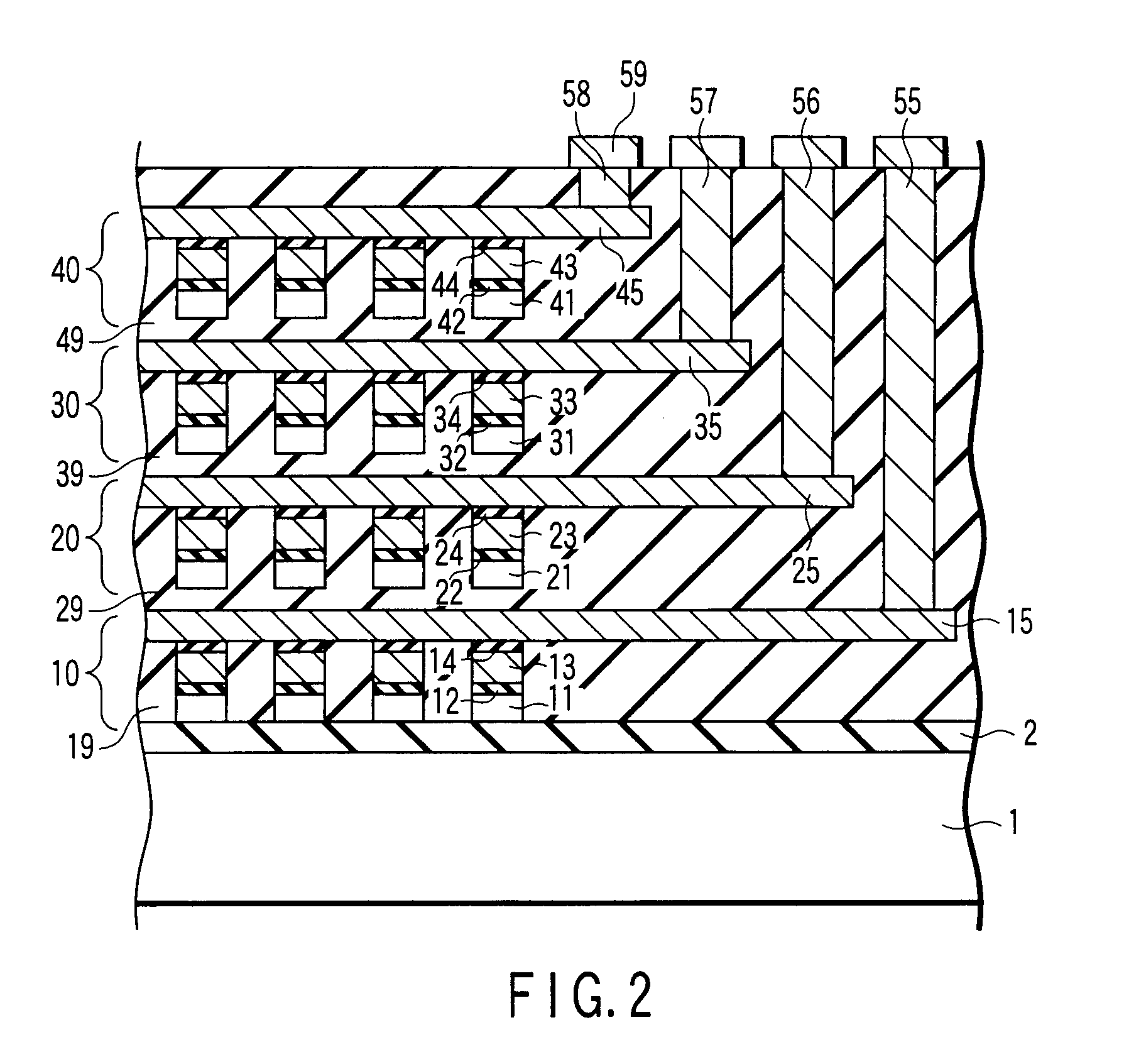
[0018]A non-volatile semiconductor storage device according to a first embodiment of the present invention is a three-dimensional non-volatile semiconductor storage device having a structure where a plurality of memory cell layers each having an SOI structure are laminated. The non-volatile semiconductor storage device according to this embodiment will now be explained hereinafter while taking an NAND-type flash memory having a double-layered gate structure having a floating gate electrode and a control gate electrode as an example. However, the embodiment is not limited to the NAND-type flash memory and may be also applied to other non-volatile semiconductor storage devices, e.g., an NOR-type flash memory and the like, a metal-oxide-nitride-oxide-silicon (MONOS) type non-volatile semiconductor storage device using a silicon nitride film (an Si3N4 film) as a charge storage layer in place of the floating gate electrode, or a tantalum nitride-aluminum oxide-oxide-nitride-oxide-silicon...

modification 1

(Modification 1)

[0034]In the first embodiment, the first memory cell array 10 is a dummy memory cell array in which the first control gate electrode 15 is just used as the back gate electrode when the second memory cell array 20 is operated. In a three-dimensional non-volatile semiconductor storage device according to Modification 1, a first memory cell array 10 is operated as an actual memory cell array like the memory cell array in the upper layer in the first embodiment. Therefore, as shown in FIG. 3, there is provided a three-dimensional semiconductor storage device in which a plurality of back gate electrodes 8 are formed in an insulator 2 below the first memory cell array 10. The back gate electrode 8 is provided to align with a corresponding first gate stack 10G. A distance between the back gate electrode 8 and the first semiconductor layer 11 is preferably controlled to, e.g., 30 to 40 nm like the distance between the first control gate electrode 15 and the second semiconduc...

second embodiment

[0036]A non-volatile semiconductor storage device according to a second embodiment of the present invention is a three-dimensional non-volatile semiconductor storage device in which every other memory cell layer has a structure turned upside down.

[0037]FIG. 4 shows an example of a cross-sectional structure of a three-dimensional NAND-type flash memory according to this embodiment. FIG. 4 depicts memory cell arrays 10, 20, 30, and 40 in four layers formed on a semiconductor substrate 1. It is to be noted that the number of the laminated layers is not limited to four and it may be smaller or larger than this value as long as it is an even number. As shown in FIG. 4, the memory cell arrays 10 and 30 in the odd-numbered layers are turned upside down to face the memory cell arrays in the even-numbered layers so that semiconductor layers 11 and 21 face each other and semiconductor layers 31 and 41 face each other. That is, for example, a gate stack 10G in the first memory cell array 10 is...


PUM


Abstract

A three-dimensional non-volatile semiconductor storage device which realizes both increased packing density and improved performance is disclosed. According to one aspect, there is provided a non-volatile semiconductor storage device comprising a first non-volatile memory cell provided on a first insulator, which includes a first semiconductor layer, and a first gate stack provided above the first semiconductor layer and including a first charge storage layer and a first control gate electrode, and a second non-volatile memory cell provided above the first non-volatile memory cell, which includes a second semiconductor layer, and a second gate stack provided above the second semiconductor layer and including a second charge storage layer and a second control gate electrode, the second gate stack being positioned to be aligned with the first gate stack, and wherein the first control gate electrode functions as a back gate electrode to the second non-volatile memory cell.

Description

CROSS-REFERENCE TO RELATED APPLICATIONS[0001]This application is based upon and claims the benefit of priority from prior Japanese Patent Application No. 2006-324471, filed Nov. 30, 2006, the entire contents of which are incorporated herein by reference.BACKGROUND OF THE INVENTION[0002]1. Field of the Invention[0003]The present invention relates to a non-volatile semiconductor storage device, and more particularly to a three-dimensional non-volatile semiconductor storage device including a charge storage layer.[0004]2. Description of the Related Art[0005]High integration and increased packing density of a semiconductor device have been realized based on a reduction in a minimum feature size. In a non-volatile semiconductor storage device, further continuously advancing a cell size of a memory cell based on a reduction in a minimum feature size is gradually becoming difficult due to restrictions imposed on its manufacturing processes and device designs. One of measures which solve th...

Claims


Application Information

Patent Timeline
IPC IPC(8): H01L29/788
CPCH01L21/8221H01L27/0688H01L27/11551H01L27/11521H01L27/11524H01L27/115H10B69/00H10B41/20H10B41/30H10B41/35
Inventor NISHIHARA, KIYOHITOARAI, FUMITAKA
Owner KK TOSHIBA
Why Eureka
Try Eureka