3D semiconductor devices and methods of fabricating same

Active Publication Date: 2012-05-17
SAMSUNG ELECTRONICS CO LTD
View PDF2 Cites 171 Cited by
  • Summary
  • Abstract
  • Description
  • Claims
  • Application Information

AI Technical Summary

Benefits of technology

[0005]Various embodiments of the inventive concept provide highly integrated semiconductor devices and methods of fabricating same. Certain embodiments of the inventive concept provide semiconductor devices configured to prospectively prevent process accidents, thereby improving fabrication yield of devices that exhibit excellent electrical characteristics. Other embodiments of the inve

Problems solved by technology

In recent years, the provision of increasingly “fine” patterns has necessitated the development and use of very expensive pattern formation equipment.
Thus, the dramatic improvements in the integra

Method used


Image

  • 3D semiconductor devices and methods of fabricating same
  • 3D semiconductor devices and methods of fabricating same
  • 3D semiconductor devices and methods of fabricating same

Examples


Embodiment Construction

[0031]Exemplary embodiments of the inventive concept will now be described in some additional detail with reference to the accompanying drawings. The inventive concept may, however, be embodied in different forms and should not be construed as being limited to only the illustrated embodiments. Rather, these embodiments are provided so that this disclosure will be thorough and complete, and will fully convey the scope of the inventive concept to those skilled in the art.

[0032]Throughout the written description and drawings, like reference numbers and labels are used to denote like or similar elements.

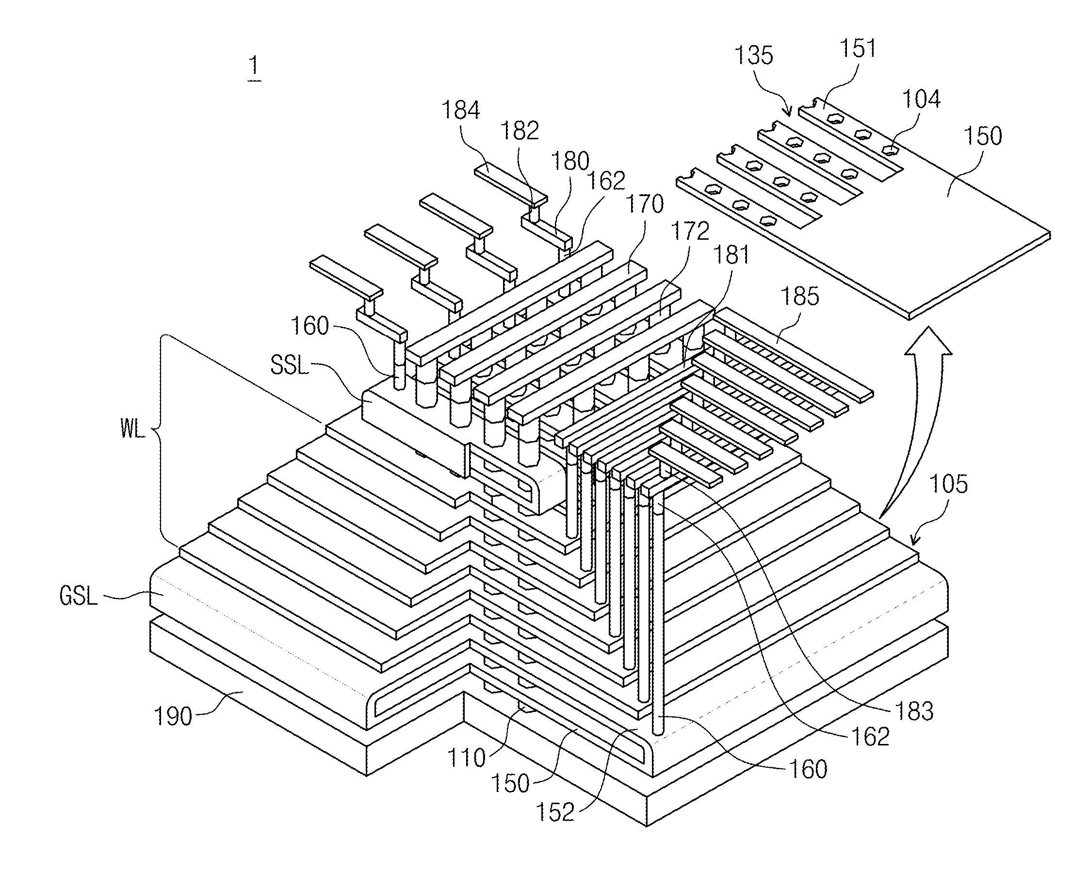
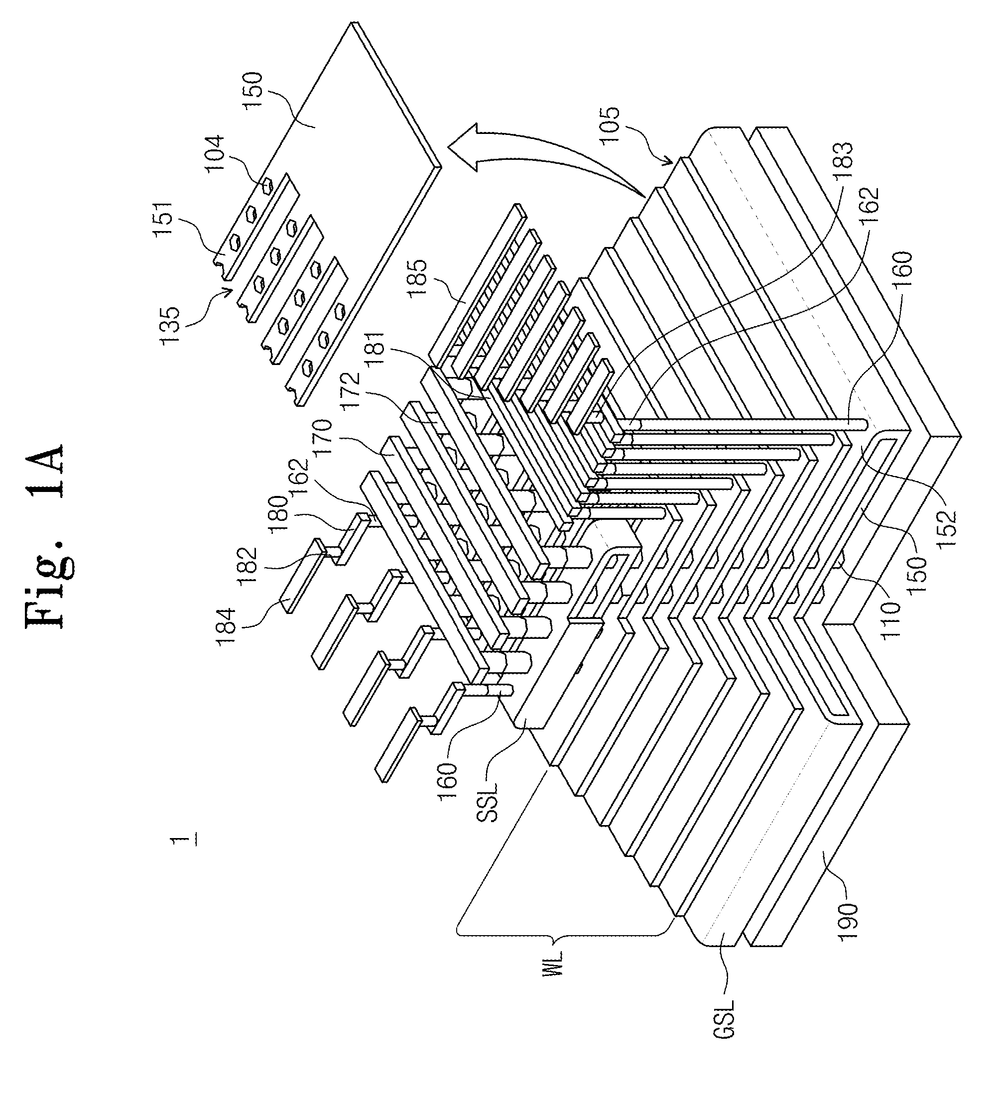
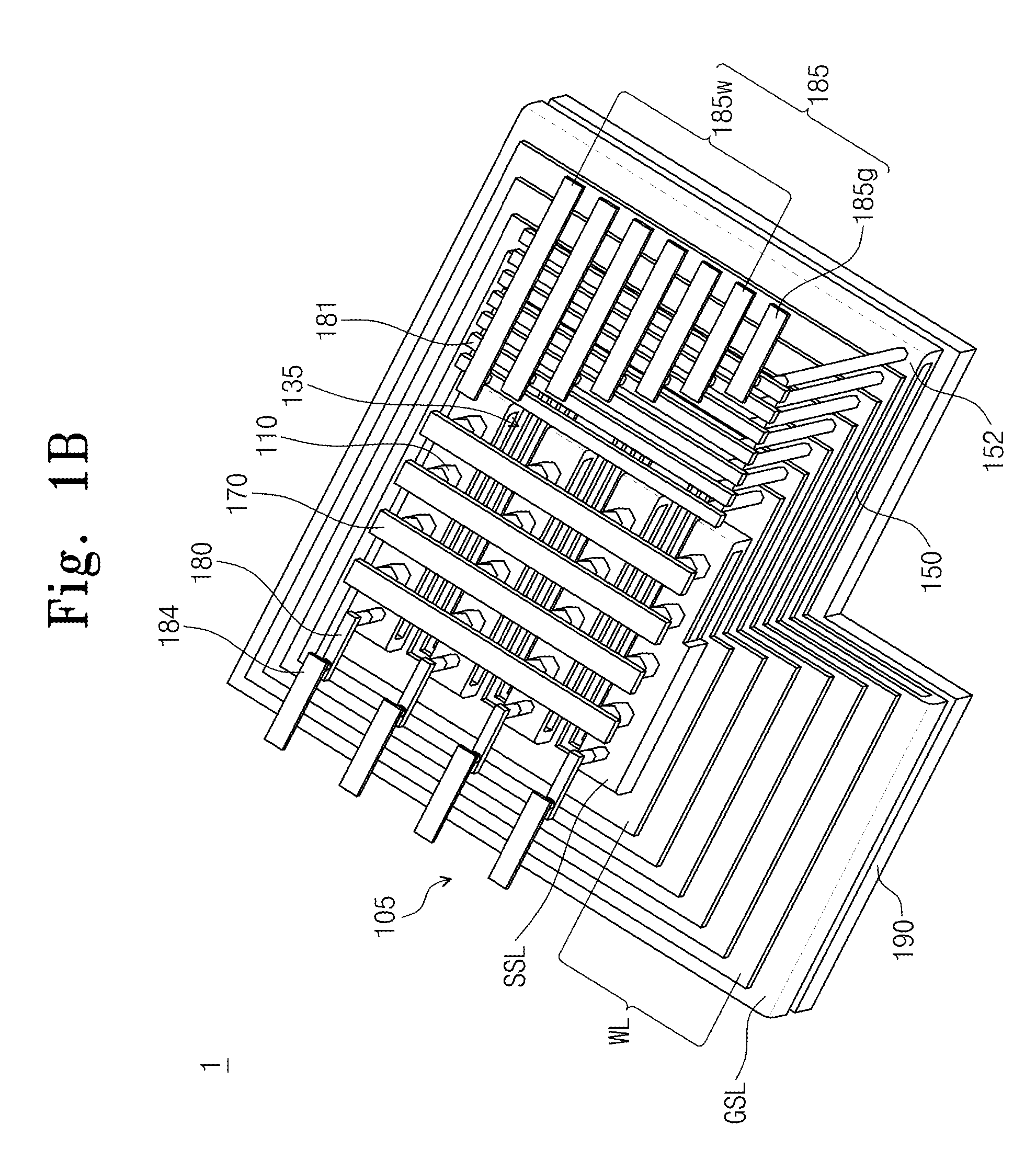
[0033]FIGS. 1A and 1B are perspective views illustrating a semiconductor device according to an embodiment of the inventive concept.

[0034]Referring to FIGS. 1A and 1B, a semiconductor device 1 may include a plurality of vertical channels 110 disposed on (extending upward from) a semiconductor substrate 190, a plurality of gates 150 constituting word lines WL and selection lines SSL and G...


PUM


Abstract

A three dimensional (3D) semiconductor device includes; a vertical channel extending from a lower end proximate a substrate to an upper end and connecting a plurality of memory cells, and a cell array comprising the plurality of cells, wherein the cell array is arranged in a gate stack of layers having a stair-stepped structure disposed on the substrate. The gate stack includes a lower layer including a lower select line coupled to a lower non-memory transistor proximate the lower end, upper layers including conductive lines respectively coupled to an upper non-memory transistor proximate the upper end and connected as a single conductive piece to form an upper select line, and intermediate layers respectively including a word line and coupled to a cell transistor, wherein the intermediate layers are disposed between the lower select line and the upper select line.

Description

CROSS-REFERENCE TO RELATED APPLICATIONS[0001]This U.S. non-provisional patent application claims priority under 35 U.S.C. §119 to Korean Patent Application No. 10-2010-0114544 filed Nov. 17, 2010, the subject matter of which is hereby incorporated by reference.BACKGROUND OF THE INVENTION[0002]The present inventive concept relates to semiconductor devices, and more particularly, to multi-layer or three dimensional (3D) semiconductor devices and methods of fabricating same.[0003]The demand for inexpensive semiconductor devices having high performance continues to drive integration density. In turn, increased integration density places greater demands on semiconductor fabrication processes. The integration density of two-dimensional (2D) or planar-type semiconductor devices is determined in part by the area occupied by the individual elements (e.g., memory cells) making up the constituent integrated circuitry. The area occupied by individual elements is largely determined by the sizing...

Claims


Application Information

Patent Timeline
IPC IPC(8): H01L29/78
CPCH01L27/11519H01L27/11548H01L27/11556H01L21/823475H01L27/11575H01L27/11582H01L29/7926H01L27/11565H10B41/10H10B41/50H10B43/10H10B43/50H10B41/27H10B43/27H01L27/0688
Inventor PARK, SANG-YONGPARK, JINTAEKKIM, HANSOOCHUNG, JUHYUCKCHO, WONSEOK
Owner SAMSUNG ELECTRONICS CO LTD
Why Eureka
Try Eureka