

Electronic device and method for fabricating the same
- Summary
- Abstract
- Description
- Claims
- Application Information
AI Technical Summary
Benefits of technology
Problems solved by technology
Method used
Image

Examples
first embodiment
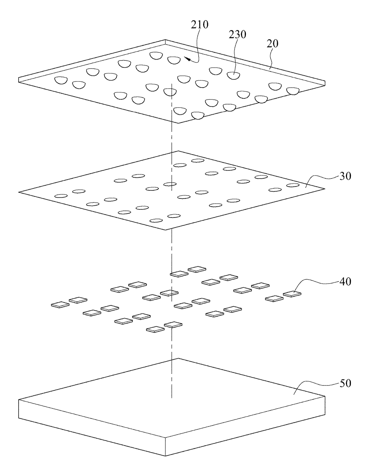
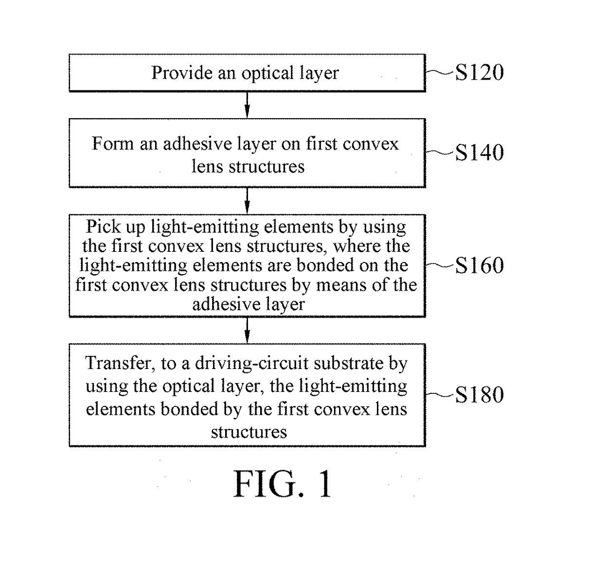
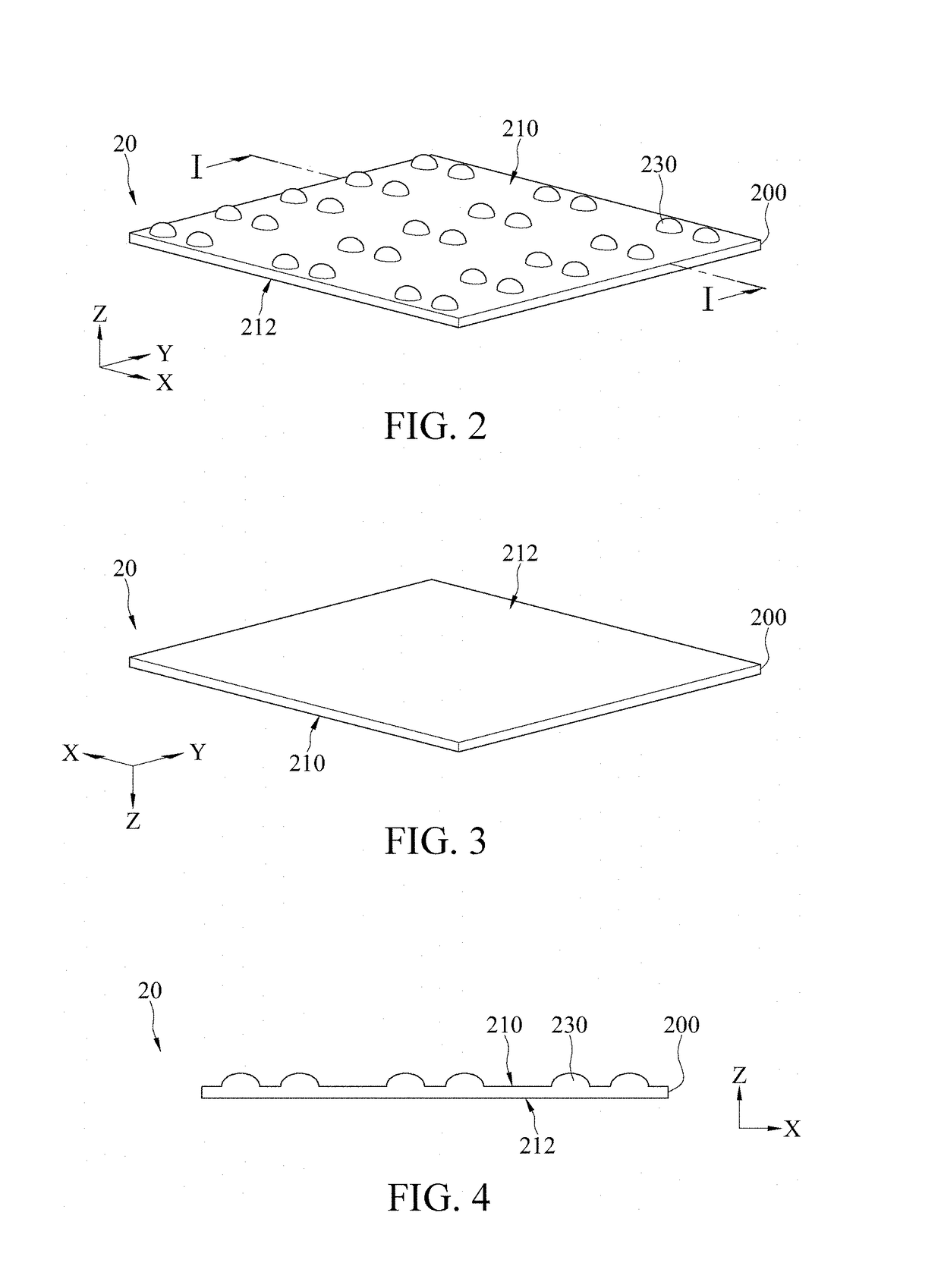
[0042]Refer to FIG. 12. FIG. 12 is a schematic diagram of an optical simulation structure of an electronic device according to the present invention. In this embodiment, the optical layer 20 is a plano convex optical layer 20. That is, the first surface 210 of the optical layer 20 has first convex lens structures 230, and the second surface 212 is a flat surface (that is, a planar structure). The material of the optical layer 20 is PDMS. FIG. 13 to FIG. 16 are diagrams of field patterns of light emission of the optical simulation structure in FIG. 12. When a radius of curvature of the first convex lens structures 230 is 28 μm (micrometer) and no glue is filled in a surrounding area 90 of the light-emitting elements 40 (that is, the surrounding area 90 is filled with air), light emitting efficiency is approximately 22.7%, as shown in FIG. 13. When the radius of curvature of the first convex lens structures 230 is 100 μm and no glue is filled in the surrounding area 90 of the light-em...
second embodiment
[0048]Refer to FIG. 21. FIG. 21 is a schematic diagram of an optical simulation structure of the electronic device according to the present invention. In this embodiment, the optical layer 20′ is a biconvex optical layer 20′. That is, a first surface 210 of the optical layer 20′ has first convex lens structures 230, and a second surface has second convex lens structures 232. In the following experiment, a material of the optical layer 20′ is PDMS and the radius of curvature of the first convex lens structures 230 is fixedly 28 μm. FIG. 22 to FIG. 25 are diagrams of field patterns of light emission of the optical simulation structure in FIG. 21. When a radius of curvature of the second convex lens structure 232 28 μm and no glue is filled in the surrounding area 90 of the light-emitting elements 40 (that is, the surrounding area 90 is filled with air), light emitting efficiency is approximately 22.4%, as shown in FIG. 22. When the radius of curvature of the second convex lens structu...
PUM
 Abstract
Description
Claims
Application Information