Fabrication method of semiconductor device and semiconductor device

Active Publication Date: 2005-05-24
RENESAS ELECTRONICS CORP +1
View PDF13 Cites 2 Cited by
  • Summary
  • Abstract
  • Description
  • Claims
  • Application Information

AI Technical Summary

Benefits of technology

[0005]With these film-forming methods, however, a silicon-germanium film is formed in high vacuum, so that the film-forming apparatus should be provided with an advanced type of vacuum pumping system. This requires a large-sized film-forming apparatus, thus increasing the fabrication costs of semiconductor device. In addition, with the case of the film formation under high vacuum, the forming speed of silicon-germanium film is relatively small. Accordingly, a long time is required for the formation of the silicon-germanium film, thereby increasing the fabrication time of semiconductor device.
[0009]Another object of the invention is to provide a fabrication method of a semiconductor device wherein a fabrication yield can be improved, and also the thus fabricated semiconductor device.
[0010]A further object of the invention is to provide a fabrication method of a semiconductor device wherein reliability can be improved, and also the thus fabricated semiconductor device.

Problems solved by technology

This requires a large-sized film-forming apparatus, thus increasing the fabrication costs of semiconductor device.
In addition, with the case of the film formation under high vacuum, the forming speed of silicon-germanium film is relatively small.
Accordingly, a long time is required for the formation of the silicon-germanium film, thereby increasing the fabrication time of semiconductor device.
In this case, although the forming speed of a silicon-germanium film can be made relatively large, a problem on practical application arises in that the productivity of semiconductor device is worsened when a thick film is formed since the condition of single wafer processing is added.
This results in the lowering in fabrication yield of the semiconductor device.

Method used


Image

  • Fabrication method of semiconductor device and semiconductor device
  • Fabrication method of semiconductor device and semiconductor device
  • Fabrication method of semiconductor device and semiconductor device

Examples


embodiment 1

(Embodiment 1)

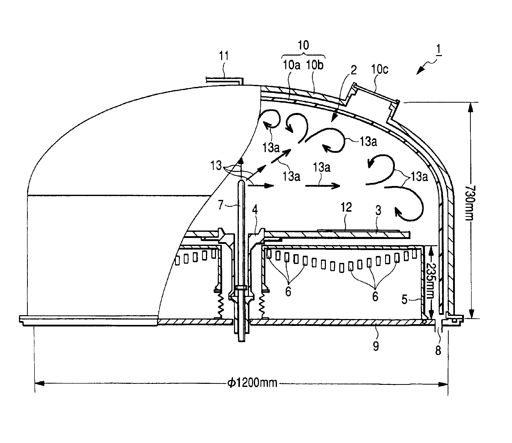
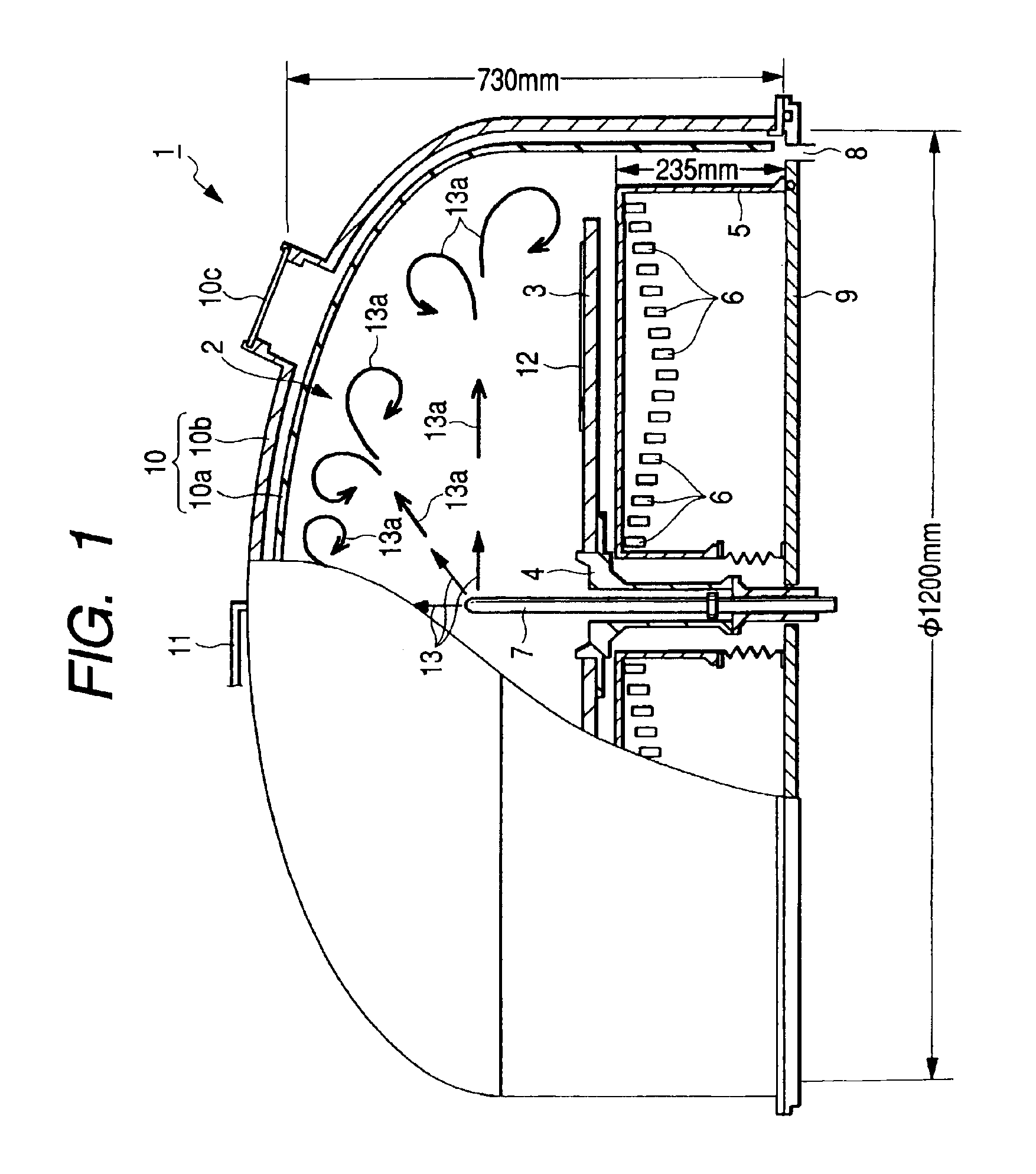
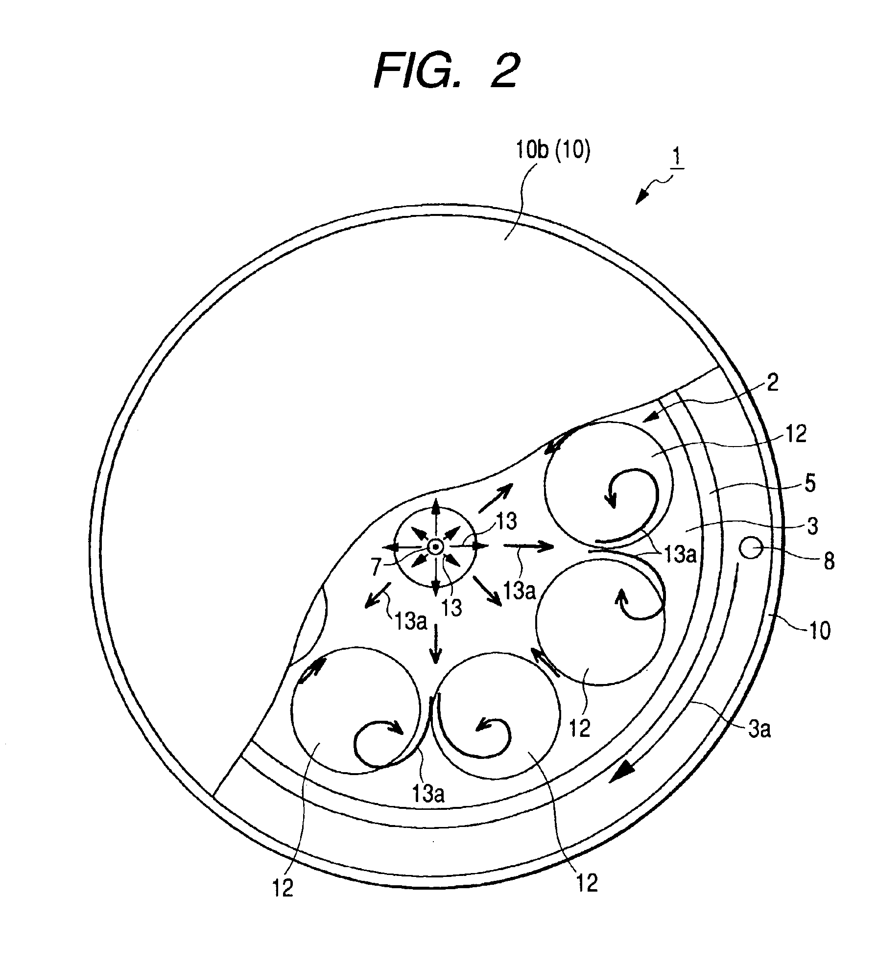
[0048]FIG. 1 is a front view, partially cut away, of a conceptional structure of a semiconductor fabricating apparatus used in the process of fabricating a semiconductor device according to this embodiment of the invention. FIG. 2 is a top view, partly cut away, of the semiconductor fabricating apparatus of FIG. 1. It will be noted that in FIG. 1, the cut away portion is shown as a conceptional section.

[0049]A semiconductor fabricating apparatus 1 shown in FIGS. 1 and 2 is a film-forming apparatus which is used in the process of forming a silicon-germanium film and a silicon film on a semiconductor substrate and is, for example, a batch-type CVD apparatus. It will be noted that for ease of understanding, structures other than a processing chamber and the inside thereof of the semiconductor fabricating device 1 are not particularly shown, with their detailed description being omitted.

[0050]The semiconductor fabricating apparatus 1 includes a reaction chamber or processi...

embodiment 2

(Embodiment 2)

[0082]FIG. 10 is a view illustrating a semiconductor fabricating apparatus used in the process of fabricating a semiconductor device according to another embodiment of the invention.

[0083]A semiconductor fabricating apparatus 41 shown in FIG. 10 is a film-forming apparatus used in the process of forming a silicon-germanium film or a silicon film on a semiconductor substrate and is a single wafer processing CVD apparatus. For understanding in a simple way, the structure of the semiconductor fabricating apparatus 41 other than a processing chamber 42 and means or members provided in the inside thereof is not particularly shown with its detailed description being omitted.

[0084]The semiconductor fabricating apparatus 41 is provided with a processing chamber 42, a susceptor 43 arranged in the processing chamber 42, a susceptor support 44 for supporting the susceptor 43, a high frequency coil 46 disposed below the susceptor and accommodated in a coil cover 45, a gas nozzle 4...

embodiment 3

(Embodiment 3)

[0093]FIG. 11 is a sectional view conceptionally showing the state wherein a silicon-germanium film 61 and a silicon film (strained silicon film) 62 are, respectively, formed on a semiconductor wafer (semiconductor substrate) 60.

[0094]The lattice constant of silicon-germanium increases with an increasing concentration of germanium. Accordingly, where the silicon-germanium film 61 is formed on the semiconductor wafer 60 made of single crystal silicon, the epitaxial growth of a silicon-germanium film having a great concentration of germanium on the semiconductor wafer 60 incurs the possibility of causing inconveniences to occur in such a way that the silicon-germanium film is greatly strained owing the difference in lattice constant thereby causing defects of high density to be formed in the silicon-germanium film. To avoid this, the concentration of germanium in the silicon-germanium film 61 is made relatively small in the vicinity of the interface between the semicondu...


PUM

PropertyMeasurementUnit
Pressureaaaaaaaaaa

Abstract

Gases for film formation are introduced from a plurality of holes provided at a gas nozzle into a processing chamber of a batch-type CVD film-forming apparatus to cause a turbulence of the gases within the processing chamber. In the state where the chamber is kept at a pressure within an atmospheric and quasi-atmospheric pressure region, a silicon-germanium film is epitaxially grown on a semiconductor wafer placed within the processing chamber. Subsequently, a strained silicon film is epitaxially grown on the silicon-germanium film. Thereafter, a semiconductor element is formed in the semiconductor wafer on which the silicon-germanium film and the strained silicon film have been formed, respectively.

Description

BACKGROUND OF THE INVENTION[0001]This invention relates to a fabrication technique of a semiconductor device and a technique for semiconductor device, and more particularly, to a fabrication method of a semiconductor device wherein a silicon germanium film is formed on a semiconductor substrate and also to a technique effective in application to semiconductor devices.[0002]In Japanese Patent Application Laid-open No. Hei 6(1994)-69131 of Ashikaga et al., a low pressure CVD method and an atmospheric pressure CVD method for the formation of an SiGe film are considered, and a novel SiGe film-forming method of overcoming the drawbacks of the former methods is proposed.SUMMARY OF THE INVENTION[0003]In recent years, speeding up of semiconductor device is in progress, and for one of approaches therefor, it has been adopted to use a silicon-germanium (SiGe) thin film. For instance, a silicon-germanium film and a silicon film are successively, epitaxially formed on a silicon substrate wherei...

Claims


Application Information

Patent Timeline
IPC IPC(8): C30B25/00H01L21/02H01L21/205C23C16/44C23C16/42C23C16/455H01L21/20H01L29/78
CPCC23C16/22H01L29/1054C23C16/45523C23C16/45563C23C16/45578C23C16/4584C23C16/46C30B25/00C30B25/02C30B29/403C30B29/52H01L21/0245H01L21/02532H01L21/02576H01L21/02579H01L21/0262H01L21/2807C23C16/45506H01L29/66575H01L29/78
Inventor KONDO, YASUICHIHIRASAWA, WATARUSUGII, NOBUYUKI
Owner RENESAS ELECTRONICS CORP
Why Eureka
Try Eureka