Method for manufacturing flexible array substrate

Active Publication Date: 2018-11-29
TCL CHINA STAR OPTOELECTRONICS TECH CO LTD
View PDF14 Cites 7 Cited by
  • Summary
  • Abstract
  • Description
  • Claims
  • Application Information

AI Technical Summary

Benefits of technology

The present invention provides a method for manufacturing a flexible array substrate that has a double-sided circuit structure. This method improves the fabrication yield of flexible array substrates by avoiding issues of poor flatness and low yield resulting from improper or wrongful re-attachment of the flexible backing plate. The method involves forming layers on a rigid support plate and then peeling off the rigid support plate and the adhesive layer to form the flexible array substrate. This method requires no steps of peeling, reversing, and then re-attaching of the flexible backing plate.

Problems solved by technology

However, due to the inevitable existence of WOA lines on a periphery of the display zone of a display panel, the distance between the display zone of the display panel and a peripheral edge is increased, making it hard to achieve bezel-free displaying or ultra-slim bezel.
Particularly, with the resolution of a display panel increasing from high definition to ultra-high definition or even higher, an increased space is necessary for disposition of the WOA lines and this makes it even harder to further narrow the bezel area.
In such a case, the GOA circuit is directly made in the non-display zone of a display panel and is directly connected to the gate lines; however, this does not allow for omission of the WOA lines, for the WOA lines are necessary for electrically connecting a drive circuit board and the GOA circuit.
The GOA circuits and the WOA lines occupy a laying area that may becomes excessively large, this being adverse to ultra-slim bezel or bezel-free displaying.
In the state of the art technology, even non laser based peeling processes, such as temperature controllable adhesives, are applied, it is still possible to cause issues of poor flatness resulting from incorrect attachment.
This makes the fabrication of the double-sided circuit structure difficult and the yield is low.

Method used


Image

  • Method for manufacturing flexible array substrate
  • Method for manufacturing flexible array substrate
  • Method for manufacturing flexible array substrate

Examples


Embodiment Construction

[0043]To further expound the technical solution adopted in the present invention and the advantages thereof, a detailed description will be given with reference to the preferred embodiments of the present invention and the drawings thereof.

[0044]Referring to FIG. 8, the present invention provides a method for manufacturing a flexible array substrate, which comprises the following steps:

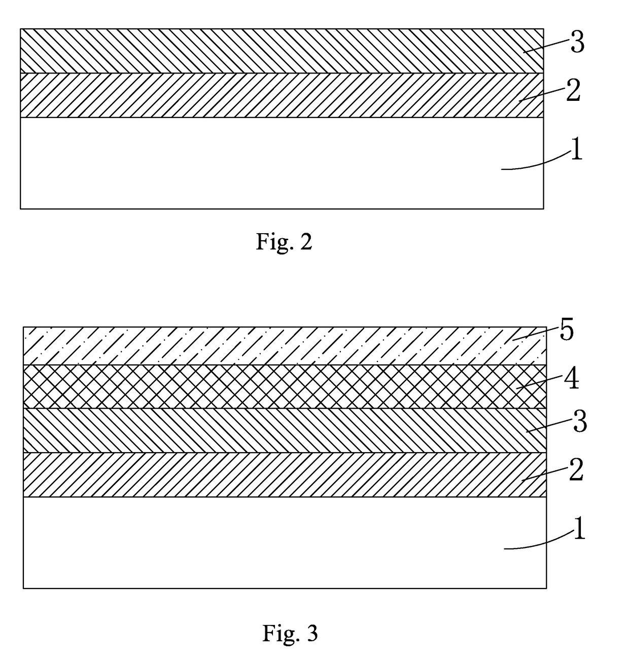
[0045]Step S1: referring to FIG. 2, providing a rigid support plate 1, forming an adhesive layer 2 on the rigid support plate 1, and forming a passivation layer 3 on the adhesive layer 2.

[0046]Specifically, the rigid support plate 1 is made of a material of glass. The adhesive layer 2 is made of an adhesive material that is selected as pressure-sensitive adhesive or temperature controllable adhesive. The passivation layer 3 is made of a material comprising an inorganic material, such as silicon oxide (SiOx) and silicon nitride (SiNx) formed through physical vapor deposition (PVD), or alternatively com...


PUM


Abstract

The present invention provides a method for manufacturing a flexible array substrate. The method includes, first, successively forming an adhesive layer, a passivation layer, a back-side drive circuit, a planarization layer, a flexible backing plate, and a front-side drive circuit and a display circuit, in a stacked arrangement, on a rigid support plate and then peeling off the rigid support plate and the adhesive layer to form a flexible array substrate having a double-sided circuit structure. The entirey process requires no steps of peeling, reversing, and then re-attaching of the flexible backing plate so that it is possible to avoid the issues of poor flatness and low yield resulting from improper or wrongful re-attachment of the flexible backing plate and thus, fabrication difficulty of a flexible array substrate having a double-sided circuit structure may be lowered down to thereby improve fabrication yield of the flexible array substrate.

Description

BACKGROUND OF THE INVENTION1. Field of the Invention[0001]The present invention relates to the field of display technology, and more particular to a method for manufacturing a flexible array substrate.2. The Related Arts[0002]With the progress of the display technology, flat panel displays, such as liquid crystal displays (LCDs) and organic light emitting diode (OLED) displays, due to various advantages, such as high image quality, low power consumption, thin device body, and wide applications, have been widely used in various consumer electronic products, such as mobile phones, televisions, personal digital assistants, digital cameras, notebook computers, and desktop computers and are now the mainstream of the display devices.[0003]Referring to FIG. 1, a known liquid crystal display generally comprises: a display panel 100, source drive chips 200 electrically connected to an upper side of the display panel 100, gate drive chips 400 electrically connected to left and right sides of ...

Claims


Application Information

Patent Timeline
IPC IPC(8): H05K3/46H05K1/11H05K3/02H05K3/40
CPCH05K3/4691H05K1/115H05K3/027H05K3/4053H05K3/025G02F1/133305G09F9/301H05K3/007H05K2201/10128G02F1/13454G02F2201/42G02F1/13452G02F1/13629G02F1/136295
Inventor CHEN, LIXUANLEE, YUNGJUI
Owner TCL CHINA STAR OPTOELECTRONICS TECH CO LTD
Why Eureka
Try Eureka