Puncture forming method, sample separating method, semiconductor element manufacturing method, semiconductor laser element manufacturing method, and semiconductor laser element

a sample separation and separating method technology, applied in semiconductor lasers, semiconductor laser structural details, manufacturing tools, etc., can solve the problems of poor the reduction of the quality of the semiconductor laser element, and achieve the effect of increasing the flatness of the separated surfa

Pending Publication Date: 2021-01-21
NUVOTON TECH CORP JAPAN
View PDF8 Cites 0 Cited by
  • Summary
  • Abstract
  • Description
  • Claims
  • Application Information

AI Technical Summary

Benefits of technology

[0007]However, the recesses formed by the conventional method provide poor flatness of the separated surface when the semiconductor laser element substrate is separated. As a result, the quality of a semiconductor laser element is also reduced.
[0008]The present disclosure has been conceived in order to solve such problems. An object of the present disclosure is to provide, for example, a puncture forming method which is capable of increasing the flatness of the separated surface when a sample, such as a semiconductor laser element substrate or a semiconductor element substrate, is separated.
[0015]According to the present disclosure, it is possible to increase the flatness of the separated surface when a sample, such as a semiconductor laser element substrate or a semiconductor element substrate, is separated.

Problems solved by technology

However, the recesses formed by the conventional method provide poor flatness of the separated surface when the semiconductor laser element substrate is separated.
As a result, the quality of a semiconductor laser element is also reduced.

Method used


Image

  • Puncture forming method, sample separating method, semiconductor element manufacturing method, semiconductor laser element manufacturing method, and semiconductor laser element
  • Puncture forming method, sample separating method, semiconductor element manufacturing method, semiconductor laser element manufacturing method, and semiconductor laser element
  • Puncture forming method, sample separating method, semiconductor element manufacturing method, semiconductor laser element manufacturing method, and semiconductor laser element

Examples


embodiment

[0050][Semiconductor Laser Element]

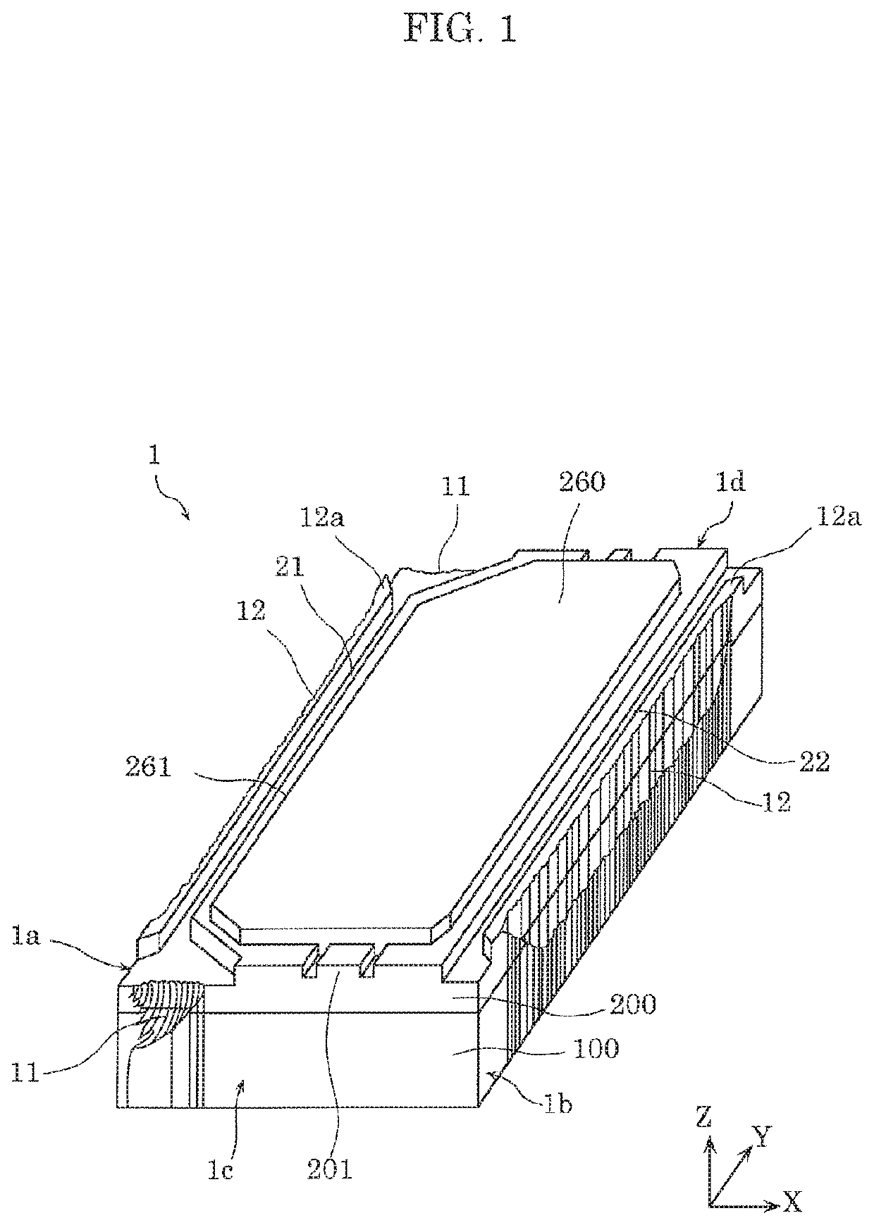
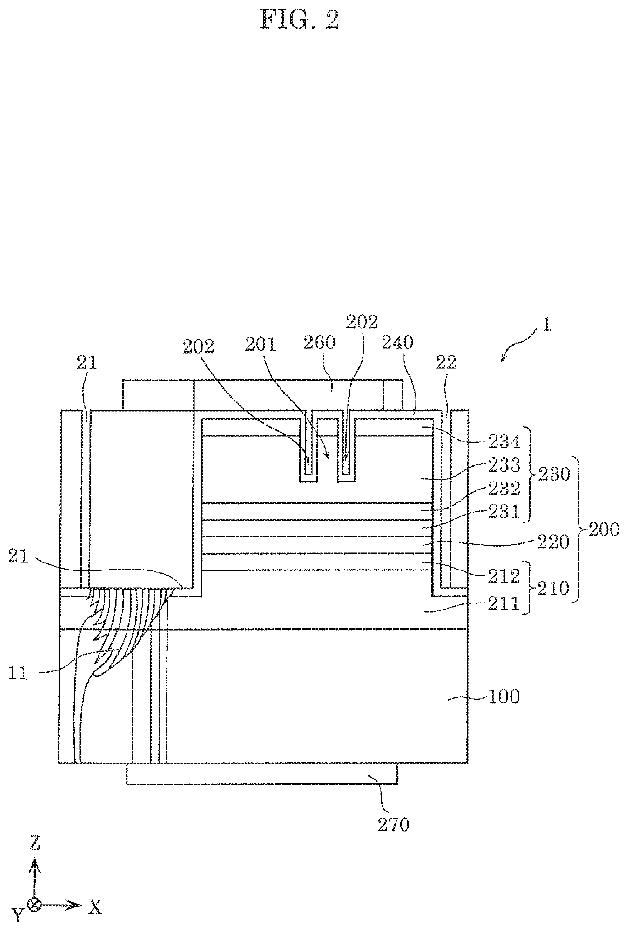
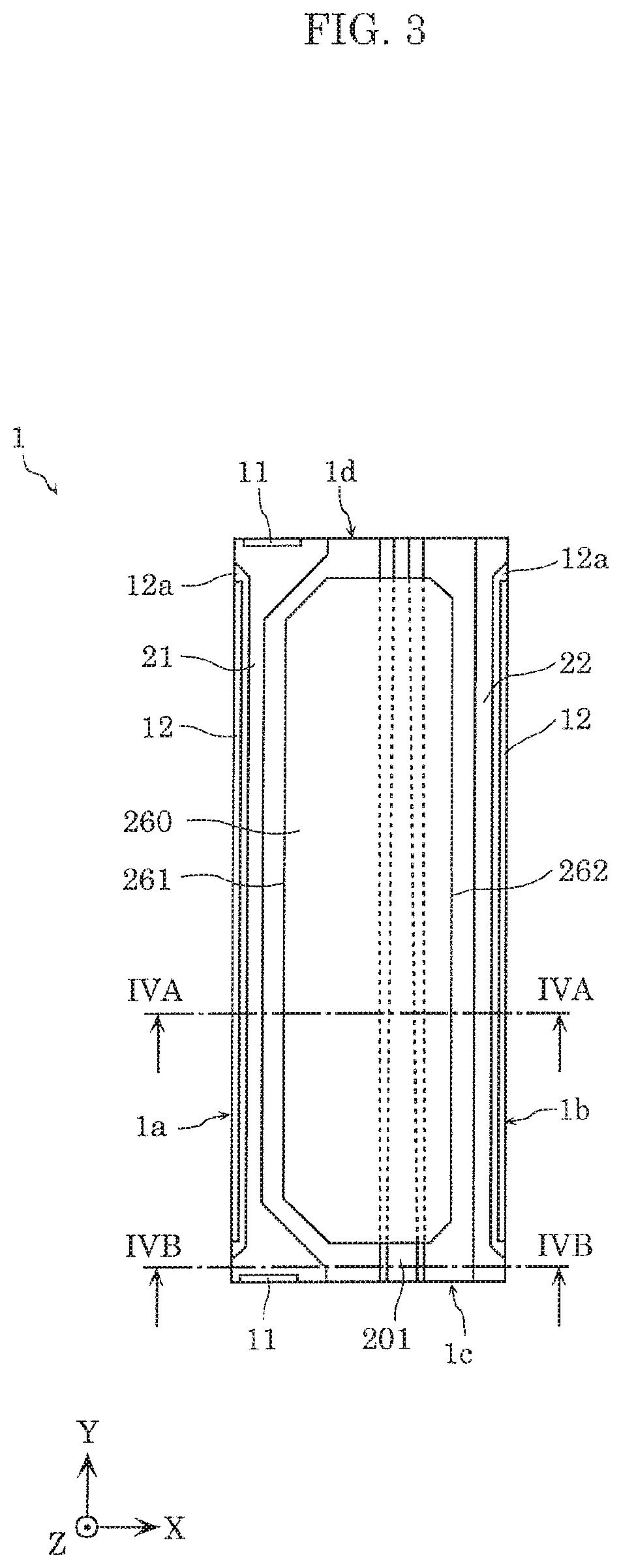
[0051]First, a configuration of semiconductor laser element 1 manufactured by a method of manufacturing semiconductor laser element 1 according to the present embodiment will be described with reference to FIG. 1 to FIG. 4B. FIG. 1 to FIG. 3 are a perspective view, a front view, and a top view of semiconductor laser element 1 according to the present embodiment, respectively. FIGS. 4A and 4B are cross-sectional views of semiconductor laser element 1 taken along lines IVA-IVA and IVB-IVB in FIG. 3, respectively.

[0052]As illustrated in FIG. 1 and FIG. 2, semiconductor laser element 1 includes first side surface 1a, second side surface 1b, third side surface 1c of (1-100) plane, and fourth side surface 1d of (˜1100) plane.

[0053]First side surface 1a and second side surface 1b are substantially parallel to the Y-axis. Specifically, first side surface 1a and second side surface 1b are substantially parallel to the YZ plane. Second side surface 1b oppose...


PUM

PropertyMeasurementUnit
thicknessaaaaaaaaaa
reflectivityaaaaaaaaaa

Abstract

A puncture forming method is a method of forming punctures in a sample by irradiating a surface of the sample with a light beam. The puncture forming method includes: forming a first puncture by irradiating a first position on the surface of the sample with a first pulse of the light beam; and after the forming of the first puncture, forming a second puncture which at least partially overlaps the first puncture by irradiating, with a second pulse of the light beam, a second position on the surface of the sample positioned away from the first position in a first direction. The second puncture has a tip which is positioned inside the sample and which is bent in a direction opposite to the first direction.

Description

CROSS REFERENCE TO RELATED APPLICATIONS[0001]This application is a U.S. continuation application of PCT International Patent Application Number PCT / JP2019 / 006876 filed on Feb. 22, 2019, claiming the benefit of priority of Japanese Patent Application Number 2018-073502 filed on Apr. 5, 2018, the entire contents of which are hereby incorporated by reference.BACKGROUND1. Technical Field[0002]The present disclosure relates to a puncture forming method, a sample separating method, a semiconductor element manufacturing method, a semiconductor laser element manufacturing method, and a semiconductor laser element, and more particularly, to a technique for forming punctures (recesses) in a sample, such as a semiconductor laser element substrate or a semiconductor element substrate, using a light beam.2. Description of the Related Art[0003]Recently, as a light source for a projector, a semiconductor light-emitting element, such as a semiconductor laser element or a light-emitting diode (LED) ...

Claims


Application Information

Patent Timeline
Patent Type & Authority Applications(United States)
IPC IPC(8): B23K26/359H01S5/02B23K26/082B23K26/0622B23K26/386
CPCB23K26/359H01S5/0201B23K2103/56B23K26/0622B23K26/386B23K26/082H01S5/0202H01S5/32341H01S5/22H01S5/04256H01L21/78
Inventor IKEDA, DAISUKEKITAGAWA, HIDEOASAKA, HIROSHIONO, MASAYUKI
Owner NUVOTON TECH CORP JAPAN
Why Eureka
Try Eureka