Semiconductor integrated circuit

a technology of integrated circuits and semiconductors, applied in semiconductor/solid-state device testing/measurement, semiconductor/solid-state device details, instruments, etc., can solve problems such as bump contact failure, conductive material failure, and various defects in the fabrication process, so as to improve the fabrication yield and reduce the test and repair time

Active Publication Date: 2013-08-15
SK HYNIX INC
View PDF5 Cites 7 Cited by
  • Summary
  • Abstract
  • Description
  • Claims
  • Application Information

AI Technical Summary

Benefits of technology

[0017]In a semiconductor integrated circuit according to an embodiment, test and repair times are reduced, resulting in the improvement of a fabrication yield.

Problems solved by technology

In the semiconductor integrated circuit using the through-silicon vias, various defects may occur in a fabrication process.
That is, there may occur defects such as void indicating that conductive material is not filled in the through-silicon via, bump contact fail due to the bending of a chip or the movement of bump material, or crack occurring in the through-silicon via.
When such defects occur, the transferring of various signals or the supply of power may not be performed among chips, resulting in a serious operation error in the semiconductor integrated circuit.
Therefore, in the semiconductor integrated circuit according to the conventional art, a test time and test-related data are increased, test efficiency is reduced due to the limitation of available channels and a memory of a test equipment, and a time for performing a repair operation is additionally necessary, resulting in a reduction in a fabrication yield of the semiconductor integrated circuit.

Method used


Image

  • Semiconductor integrated circuit
  • Semiconductor integrated circuit
  • Semiconductor integrated circuit

Examples


Embodiment Construction

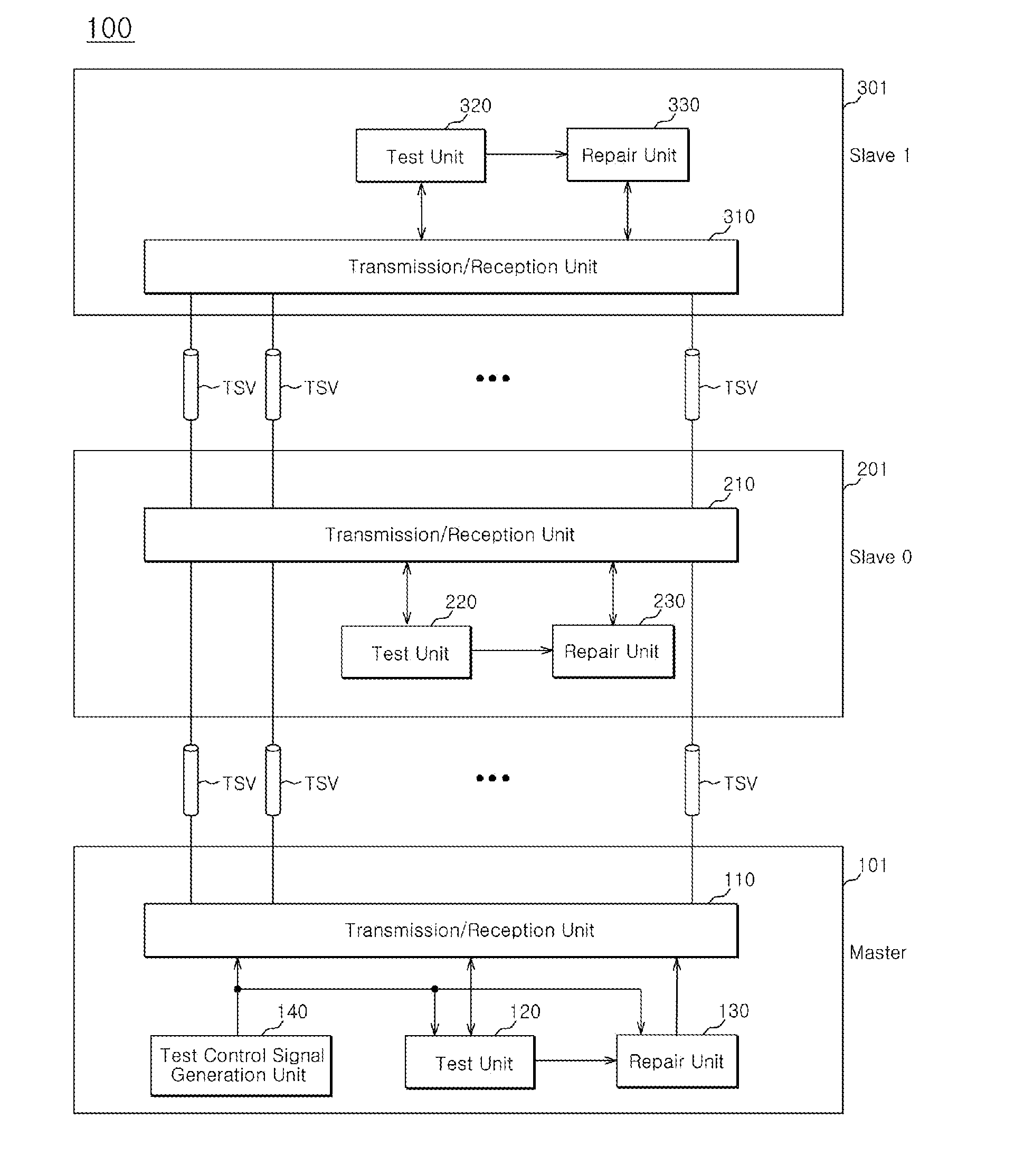
[0025]Hereinafter, a semiconductor integrated circuit according to the present invention will be described in detail with reference to the accompanying drawings through various embodiments.

[0026]First, a semiconductor integrated circuit according to an embodiment is summarized in that self-test and repair is possible.

[0027]As illustrated in FIG. 1, a semiconductor integrated circuit 100 according to an embodiment may be configured by stacking a plurality of chips, that is, a master 101, a slave 0 (201), and a slave 1 (301).

[0028]The master 101, the slave 0 (201), and the slave 1 (301) may be coupled to one another through a plurality of through-silicon vias (TSV) (hereinafter, referred to as vias).

[0029]The plurality of vias may be classified into normal vias, repair vias, and dedicated vias according to the purpose thereof.

[0030]The normal vias may be used to transmit normal operation-related signals, for example, commands, data, addresses and the like.

[0031]The repair vias may be ...


PUM


Abstract

A semiconductor integrated circuit includes a plurality of semiconductor chips coupled to one another through vias, wherein a lowermost semiconductor chip of the plurality of semiconductor chips is configured to generate a first test pulse signal and transmit the first test pulse signal through the via, an uppermost semiconductor chip of the plurality of semiconductor chips is configured to generate a second test pulse signal while substantially maintaining a time difference with the first test pulse signal, and to transmit the second test pulse signal through the via, and the plurality of semiconductor chips are configured to generate test result signals for determining whether the vias are defective in response to the first test pulse signal and the second test pulse signal.

Description

CROSS-REFERENCES TO RELATED APPLICATION[0001]The present application claims priority under 35 U.S.C. §119(a) to Korean application number 10-2012-0014856, filed on Feb. 14, 2012, in the Korean Intellectual Property Office, which is incorporated herein by reference in its entirety as set forth in full.BACKGROUND[0002]1. Technical Field[0003]The present invention generally relates to a semiconductor circuit, and more particularly, to a semiconductor integrated circuit.[0004]2. Related Art[0005]Semiconductor integrated circuits are fabricated by stacking a plurality of chips in order to improve the degree of integration.[0006]As one of them, research into a via, for example, a through-silicon via (TSV) semiconductor integrated circuit has been actively conducted.[0007]According to such a method, the plurality of chips are stacked and through-silicon vias are formed, so that all the chips are coupled to one another.[0008]In the semiconductor integrated circuit using the through-silicon ...

Claims


Application Information

Patent Timeline
Patent Type & Authority Applications(United States)
IPC IPC(8): G01R31/26
CPCH01L23/481H01L22/22G01R31/318513G01R31/2853G01R31/31717H01L2924/0002H01L2924/00012H01L2924/00G01R31/3183
Inventor KU, YOUNG JUN
Owner SK HYNIX INC
Why Eureka
Try Eureka