Light emitting diode and fabricating method thereof

a technology of light-emitting diodes and fabrication methods, which is applied in the direction of semiconductor devices, basic electric elements, electrical equipment, etc., can solve the problems of compromising the fabricating yield of the led and the difficult to achieve the fabricating process so as to improve the fabricating yield of the wire bonding of the led and the light-emitting area of the led

Inactive Publication Date: 2008-05-29
FORMOSA EPITAXY INCORPORATION
View PDF9 Cites 9 Cited by
  • Summary
  • Abstract
  • Description
  • Claims
  • Application Information

AI Technical Summary

Benefits of technology

[0008]Accordingly, the present invention is directed to provide an LED having big areas for the light emitting layer and electrode simultaneously, so that the lighting area of the LED can be increased and the fabricating yield of the wire bonding of the LED is improved.

Problems solved by technology

However, when the area of the electrode 122 is too small, the difficulty of fabricating process of the wire bonding may increase; further, the fabricating yield of the LED is compromised.

Method used


Image

  • Light emitting diode and fabricating method thereof
  • Light emitting diode and fabricating method thereof
  • Light emitting diode and fabricating method thereof

Examples


Embodiment Construction

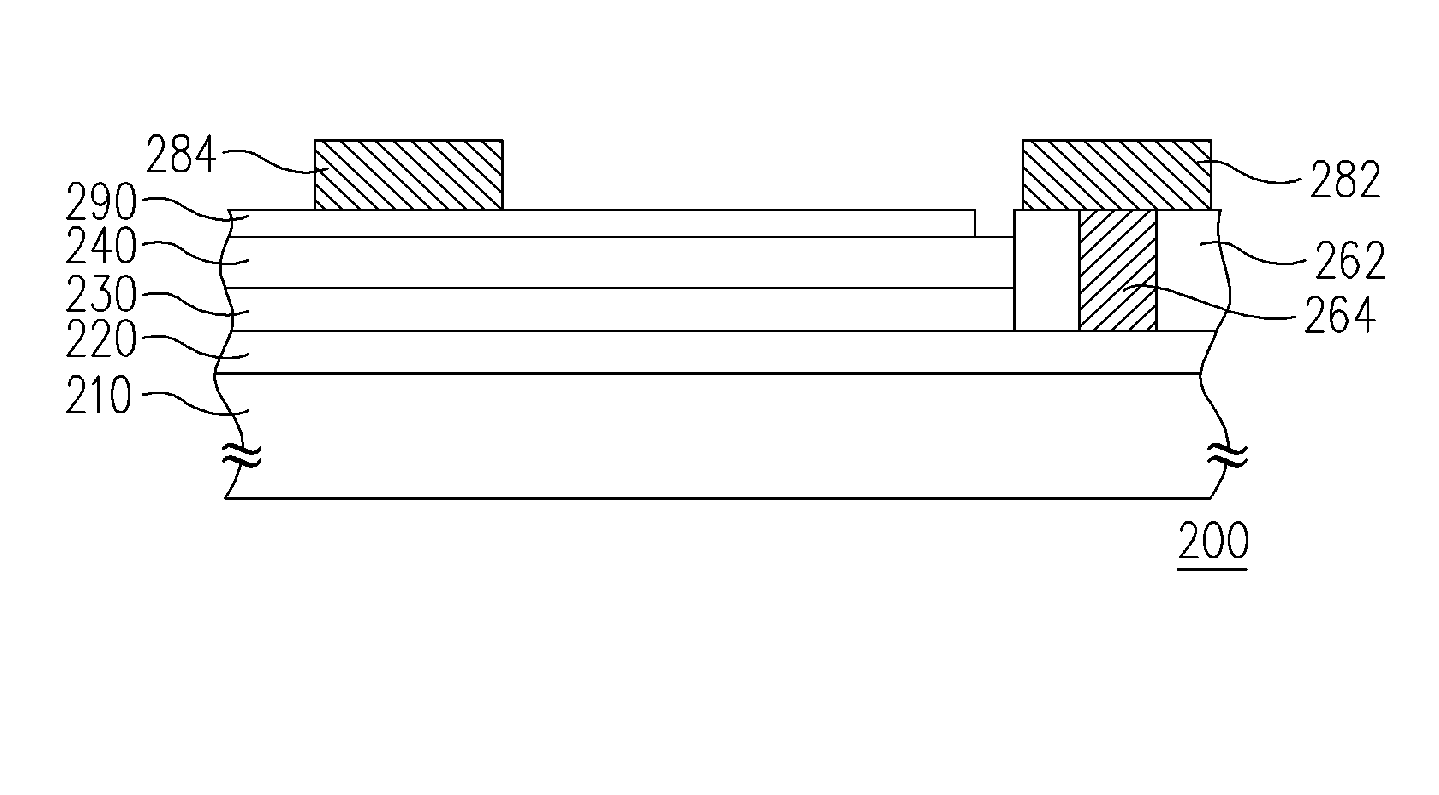
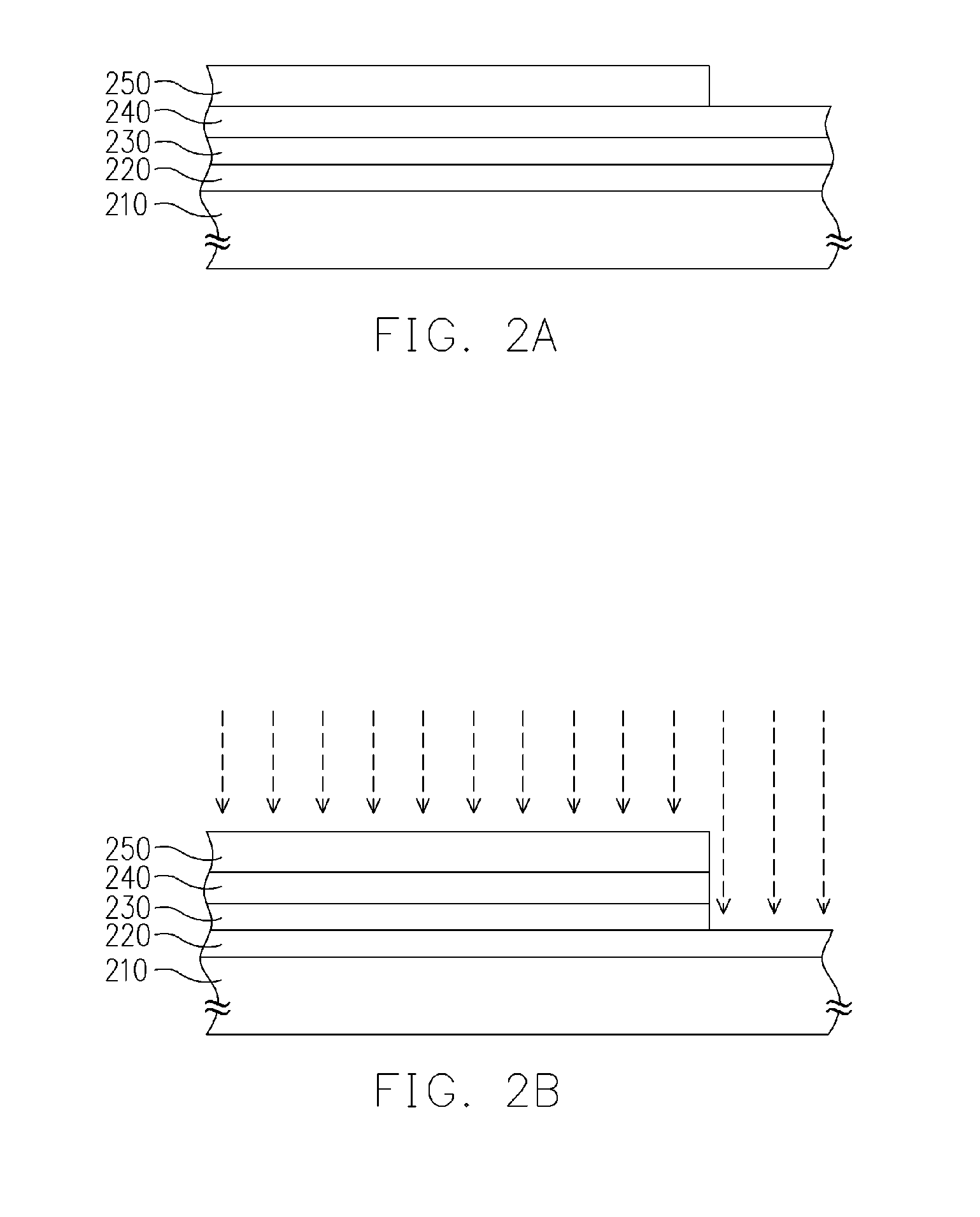
[0033]FIGS. 2A to 2F are schematic cross-sectional fabricating flow charts of the LED according to the embodiment of the present invention. Referring to FIG. 2A, first, a first type doping semiconductor layer 220, a light emitting layer 230, a second type doping semiconductor layer 240 and a mask layer 250 are formed on the substrate 210 in sequence. Wherein, the mask layer 250 exposes a portion of the second type doping semiconductor layer 240.

[0034]As above, the material of the substrate 210 is, for example, sapphire, carborundum, spinel or silicon. The materials of the first type doping semiconductor layer 220, the light emitting layer 230 and the second type doping semiconductor layer 240 are, for example, III-V compound semiconductor material, and the most common materials used are GaN, GaAlN or GalnN. In the embodiment, the first type doping semiconductor layer 220 is, for example, an n-type doping semiconductor layer, and the second type doping semiconductor layer 240 is, for...


PUM


Abstract

An LED includes a substrate, a first type doping semiconductor layer, a first electrode, a light emitting layer, a second type doping semiconductor layer, a second electrode, a first dielectric layer and a first conductive plug. The first type doping semiconductor layer is formed on the substrate, and the light emitting layer, the second type doping semiconductor layer and the second electrode are formed on a portion of the first type doping semiconductor layer in sequence. The first dielectric layer is formed on another portion of the first type doping semiconductor layer where is not covered by the light emitting layer. The first electrode formed on the first dielectric layer is electrically connected with the first type doping semiconductor layer through the first conductive plug formed in the first dielectric layer. Furthermore, the second electrode is electrically connected with the second type doping semiconductor layer.

Description

BACKGROUND OF THE INVENTION[0001]1. Field of Invention[0002]The present invention relates to a light emitting device and fabricating method thereof. More particularly, the present invention relates to a light emitting diode (LED) and fabricating method thereof.[0003]2. Description of Related Art[0004]Compared with a conventional bulb, the light emitting diode (LED) has outstanding advantages, such as compact, long-life, low driving voltage / current, cracking resistance, no obvious thermal problem when lighting, mercury free (no pollution problem), high lighting efficiency (power saving), etc. In addition, the lighting efficiency of LEDs has been continuously improved in recent years. Hence, LEDs have gradually replaced fluorescent lamps and incandescent lamps in some fields, such as the scanner light source, the back or front light of the liquid crystal display, the illumination for the instrument panel of automobile, the traffic signal lamps and the general lighting devices.[0005]Fu...

Claims


Application Information

Patent Timeline
Patent Type & Authority Applications(United States)
IPC IPC(8): H01L33/00H01L33/32H01L33/38H01L33/44
CPCH01L33/32H01L2933/0016H01L33/44H01L33/38
Inventor WEN, WAY-JZELIN, YI-FONGTSENG, HUAN-CHEPAN, SHYI-MINGCHIEN, FEN-RENHUANG, KUO-RUEISONG, WEN-JOE
Owner FORMOSA EPITAXY INCORPORATION
Why Eureka
Try Eureka