Semiconductor Optical Element and Manufacturing Method Thereof

a technology of semiconductor and optical elements, applied in semiconductor devices, lasers, semiconductor lasers, etc., to achieve the effect of enhancing fabrication yield and excellent device characteristics

Active Publication Date: 2008-06-12
NIPPON TELEGRAPH & TELEPHONE CORP
View PDF6 Cites 6 Cited by
  • Summary
  • Abstract
  • Description
  • Claims
  • Application Information

AI Technical Summary

Benefits of technology

[0013]There is encountered such a problem that the concavo-convex shape before the growth of the contact layer, i.e., after the growth of the over-cladding layer must be flattened so as not to cause a problem in the crystal quality of the contact layer in order to provide the excellent device characteristics and enhance the fabrication yield and the run-to-run reproducibility in the buried structure using a low mesa on the p-type substrate.

Problems solved by technology

There is encountered such a problem that the concavo-convex shape before the growth of the contact layer, i.e., after the growth of the over-cladding layer must be flattened so as not to cause a problem in the crystal quality of the contact layer in order to provide the excellent device characteristics and enhance the fabrication yield and the run-to-run reproducibility in the buried structure using a low mesa on the p-type substrate.

Method used


Image

  • Semiconductor Optical Element and Manufacturing Method Thereof
  • Semiconductor Optical Element and Manufacturing Method Thereof
  • Semiconductor Optical Element and Manufacturing Method Thereof

Examples


embodiment 1

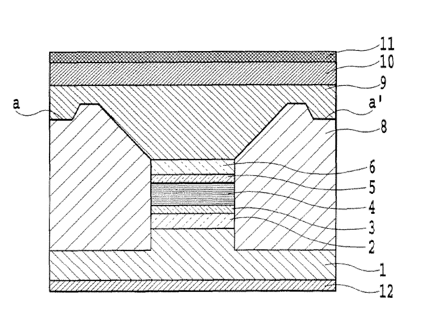
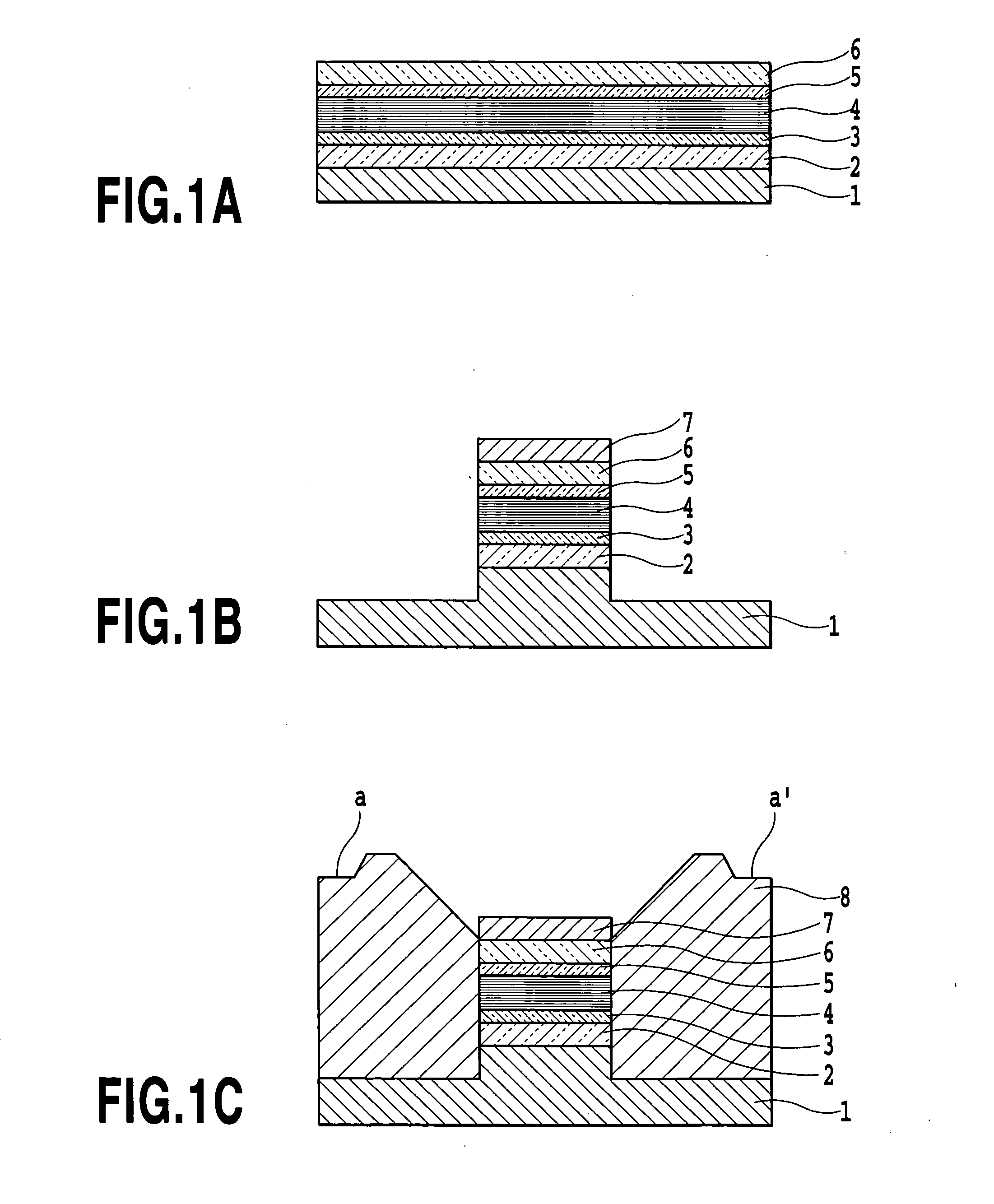
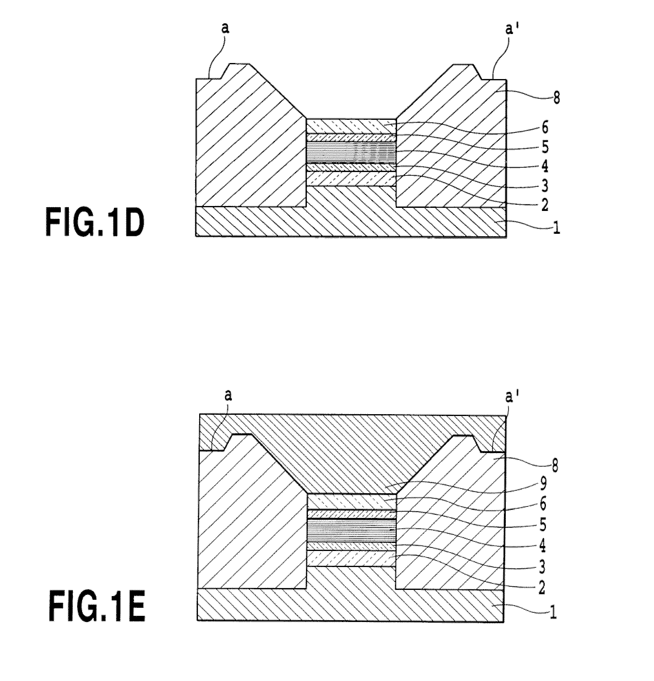
[0047]FIGS. 1A to 1G show processes for fabricating a semiconductor device according to a first embodiment of the present invention. These figures are cross sectional views of a directly modulated semiconductor DFB laser using an MQW as an active layer. Firstly, as shown in FIG. 1A, a Zn-doped p-type InP cladding layer 2 having a layer thickness of 0.5 μm, a nondoped-InGaAsP lower separate confinement heterostructure (SCH) layer 3 having a layer thickness of 0.05 μm, a non-doped InGaAsP / InGaAsP strain multiple quantum well (MQW) active layer 4 having a layer thickness of 0.15 μm and having a bandgap wavelength of 1.3 μm, and a non-doped InGaAsP upper separate confinement heterostructure (SCH) layer 5 having a layer thickness of 0.05 μm were grown in order on a Zn-doped p-type InP substrate 1 having surface orientation (100) by utilizing a metal organic vapor-phase epitaxy (MOVPE) method. After a diffraction grating was formed on an upper portion of the InGaAsP upper separate confine...

embodiment 2

[0063]FIGS. 4A to 4G show processes for fabricating a semiconductor device according to a second embodiment of the present invention. These figures are cross sectional views showing a directly modulated semiconductor DFB laser having an MQW as an active layer. Firstly, as shown in FIG. 4A, a Zn-doped n-type InP cladding layer 22 having a layer thickness of 0.5 μm, a nondoped-InGaAsP lower separate confinement heterostructure (SCH) layer 23 having a layer thickness of 0.05 μm, a nondoped-InGaAsP / InGaAsP strain multiple quantum well (MQW) active layer 24 having a layer thickness of 0.15 μm and having a bandgap wavelength of 1.3 μm, and a nondoped-InGaAsP upper separate confinement heterostructure (SCH) layer 25 having a layer thickness of 0.05 μm were grown in order on a Zn-doped p-type InP substrate 21 having surface orientation (100) by utilizing the metal organic vapor-phase epitaxy (MOVPE) method. After a diffraction grating was formed on an upper portion of the InGaAsP upper sepa...

embodiment 3

[0069]FIGS. 5A to 5G show processes for fabricating a semiconductor device according to a third embodiment of the present invention. These figures are cross sectional views of a directly modulated semiconductor DFB laser having an MQW as an active layer. Firstly, as shown in FIG. 5A, a Zn-doped p-type InP cladding layer 42 having a layer thickness of 0.5 μm, a nondoped-InGaAsP lower separate confinement heterostructure (SCH) layer 43 having a layer thickness of 0.05 μm, a nondoped-InGaAsP / InGaAsP strain multiple quantum well (MQW) active layer 44 having a layer thickness of 0.15 μm and having a bandgap wavelength of 1.3 μm, and a nondoped-InGaAsP upper separate confinement heterostructure (SCH) layer 45 having a layer thickness of 0.05 μm were successively grown on a Zn-doped p-type InP substrate 41 having surface orientation (100) by utilizing the metal organic vapor-phase epitaxy (MOVPE) method. After a diffraction grating was formed on an upper portion of the InGaAsP upper separa...


PUM


Abstract

In order to provide excellent device characteristics and enhance fabrication yield and run-to-run reproducibility in a buried device structure using a low mesa on a p-type substrate, a cross sectional configuration before growth of a contact layer of a device, i.e., after growth of an over-cladding layer is flattened so as not to cause a problem in crystal quality of the contact layer. A mesa-stripe stacked body including at least a p-type cladding layer (2), an active layer (4) and an n-type cladding layer (6) is formed on a p-type semiconductor substrate (1), a current-blocking layer (8) is buried in both sides of the stacked body, and an n-type over-cladding layer (9) and an n-type contact layer (10) are disposed on the current-blocking layer (8) and the stacked body. The n-type over-cladding layer (9) is made of a semiconductor crystal having a property for flattening a concavo-convex shape of upper surfaces of the current-blocking layer (8) and the stacked body.

Description

TECHNICAL FIELD[0001]The present invention relates to a semiconductor optical device and a method of fabricating the same.BACKGROUND ART[0002]A buried structure having a semiconductor crystal as a current-blocking burying layer is used in a semiconductor optical device such as a semiconductor laser. This structure is very important in the practical use of a device because it has advantages such as reduction in threshold current of a semiconductor laser due to a good current-blocking, stabilization of an optical beam by transverse mode control, good heat dissipation from an active layer due to a semiconductor burying layer, and high long-term reliability.[0003]A directly modulated laser which is one of components necessary for a large capacity optical transmission system is an important component as a light source of a middle / short-distance high speed optical transmission system. Thus, reduction in cost is strongly required for the directly modulated laser. More specifically, in orde...

Claims


Application Information

Patent Timeline
Patent Type & Authority Applications(United States)
IPC IPC(8): H01S5/227H01L33/00H01S5/12
CPCB82Y20/00H01S5/0265H01S5/12H01S5/2224H01S5/3434H01S5/227H01S5/2275H01S5/305H01S5/3072H01S5/2226
Inventor IGA, RYUZOKONDO, YASUHIRO
Owner NIPPON TELEGRAPH & TELEPHONE CORP
Why Eureka
Try Eureka