Asymmetric band-gap engineered nonvolatile memory device

a nonvolatile, band-gap technology, applied in semiconductor devices, digital storage, instruments, etc., can solve the problems of silicon not readily diffused within si.sub.3 n.sub.4 and relatively weak mechanism

Inactive Publication Date: 2004-08-31
MICRON TECH INC
View PDF41 Cites 191 Cited by
  • Summary
  • Abstract
  • Description
  • Claims
  • Application Information

AI Technical Summary

Problems solved by technology

But this mechanism is relatively weak due to the low field (k<0.5) between the floating gate and the substrate.
Silicon readily diffuses within silicon oxide at elevated processing temperatures, which disrupts the injection threshold by reducing the localized field distortions.
However, even at higher processing temperature, silicon does not readily diffuse within Si.sub.3 N.sub.4.
The low efficiency is attributable to the geometry and capacitor divider effects of the cell.

Method used


Image

  • Asymmetric band-gap engineered nonvolatile memory device
  • Asymmetric band-gap engineered nonvolatile memory device
  • Asymmetric band-gap engineered nonvolatile memory device

Examples


Embodiment Construction

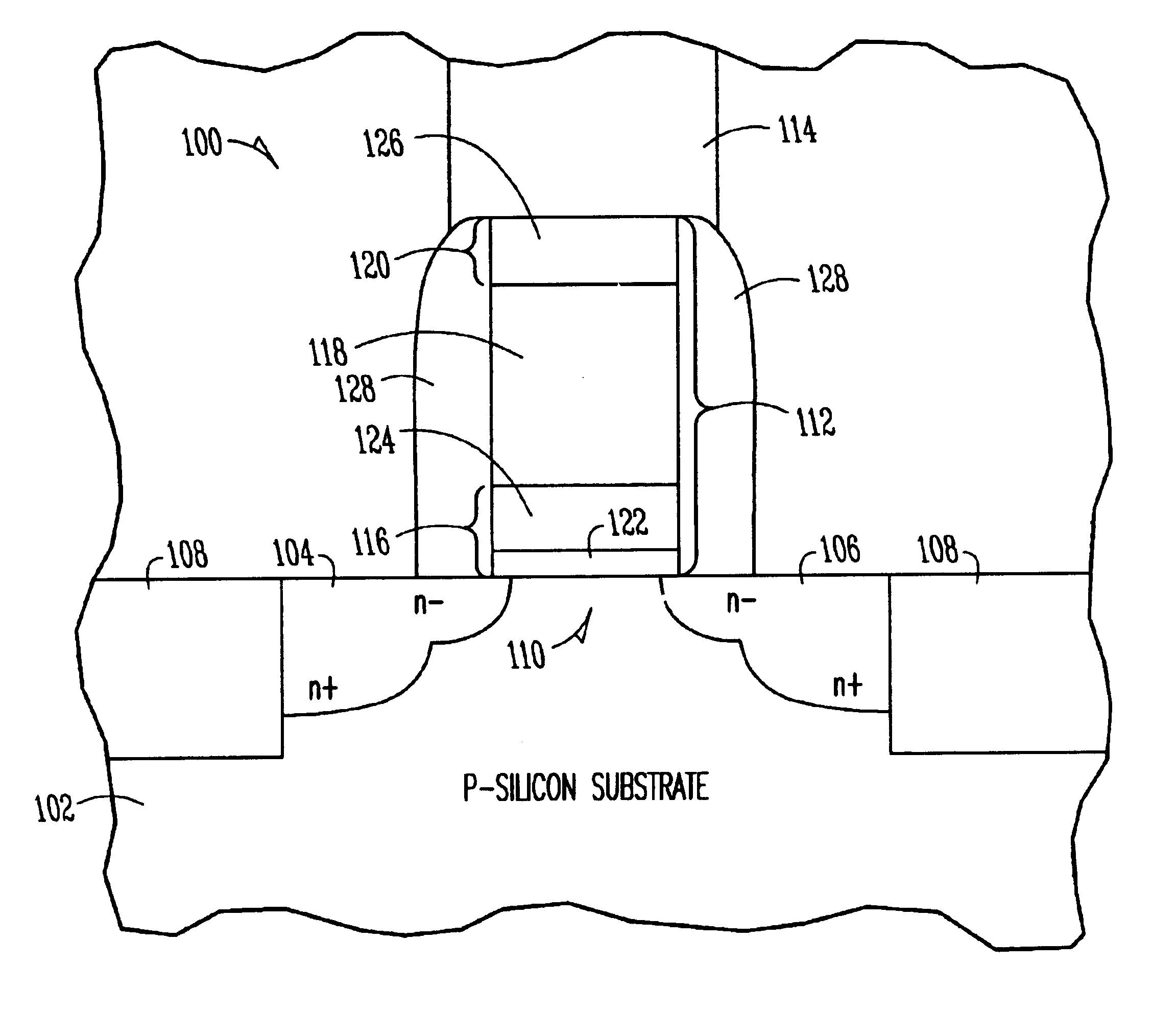
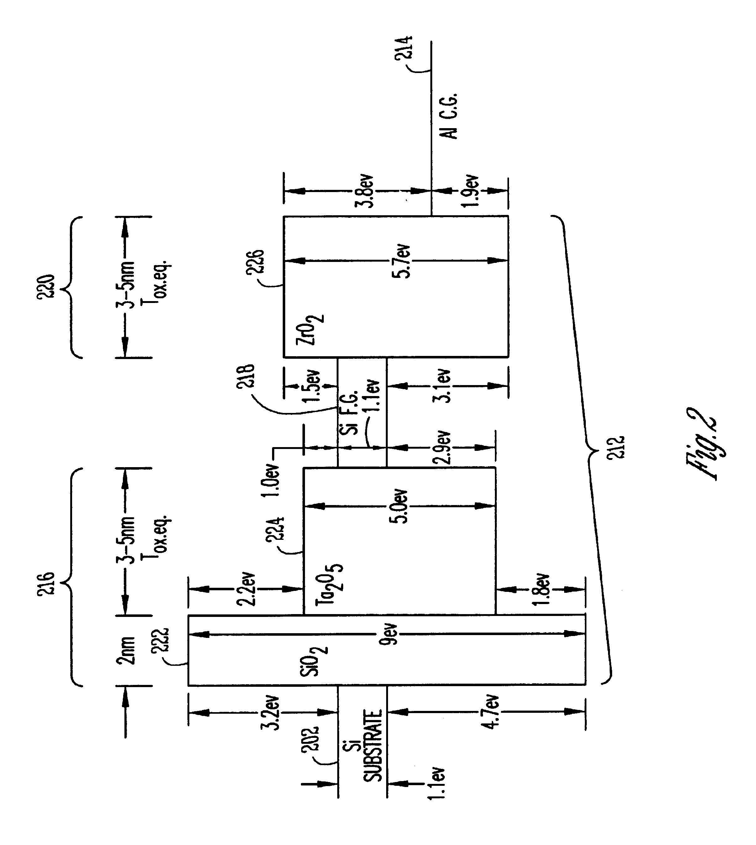
refers to the accompanying drawings which show, by way of illustration, specific aspects and embodiments in which the invention may be practiced. In the drawings, like numerals describe substantially similar components throughout the several views. These embodiments are described in sufficient detail to enable those skilled in the art to practice the invention. Other embodiments may be utilized and structural, logical, and electrical changes may be made without departing from the scope of the present invention. In the following description, the terms wafer and substrate are interchangeably used to refer generally to any structure on which integrated circuits are formed, and also to such structures during various stages of integrated circuit fabrication. Both terms include doped and undoped semiconductors, epitaxial layers of a semiconductor on a supporting semiconductor or insulating material, combinations of such layers, as well as other such structures that are known in the art. T...


PUM


Abstract

Systems and methods are provided for nonvolatile memory devices that incorporate a band-gap engineered gate stack with asymmetric tunnel barriers. One embodiment of a memory device includes first and second source / drain regions separated by a channel region in a substrate, a control gate, and a gate stack between the control gate and the channel region. The gate stack includes a first insulator region in contact with the channel region, a floating charge-storage region in contact with the first insulator region, and a second insulator region in contact with the floating charge-storage region and the control gate. The gate stack includes selected material, in conjunction with control gate metallurgy, for providing desired asymmetric energy barriers that are adapted to primarily restrict carrier flow during programming to a selected carrier between the control gate and the floating charge-storage region, and to retain a programmed charge in the floating charge-storage region. Other aspects are provided herein.

Description

This invention relates generally to integrated circuits and, more particularly, to nonvolatile programmable memory cells.Conventional nonvolatile flash and Electronically Erasable Programmable Read Only Memory (EEPROM) devices are "dual-threshold" Field Effect Transistor (FET) devices. These devices include a floating silicon gate ("floating gate") isolated from the top programming gate ("control gate"). These devices are programmed (write and / or erase) by applying a set of programming potentials between the control gate and the silicon substrate. Devices are read as being either in the nonconducting state or in the conducting state based on the threshold state of the FET device. Hot carriers, which are usually electrons, are conventionally supplied and injected from the silicon substrate. Electrons are collected by the floating gate to raise the threshold to the nonconducting state for an NFET device and conversely discharged into the substrate to lower the threshold and return to ...

Claims


Application Information

Patent Timeline
Patent Type & Authority Patents(United States)
IPC IPC(8): H01L29/423H01L21/28H01L21/02H01L29/40G11C16/04G11C8/02G11C16/10
CPCG11C16/10H01L21/28273H01L29/42332H01L29/42348G11C16/0416H01L29/40114
Inventor BHATTACHARYYA, ARUP
Owner MICRON TECH INC
Why Eureka
Try Eureka