Multi-level Lateral Floating Coupled Capacitor Transistor Structures

a coupled capacitor and transistor technology, applied in the direction of basic electric elements, electrical equipment, semiconductor devices, etc., can solve the problems of reducing the breakdown voltage, reducing the amount of current flow, and reducing the use of drift region doping concentrations to adjust the on-resistance and breakdown voltage. , to achieve the effect of reducing on-resistance and higher breakdown voltag

Active Publication Date: 2010-05-20
SEMICON COMPONENTS IND LLC
View PDF10 Cites 17 Cited by
  • Summary
  • Abstract
  • Description
  • Claims
  • Application Information

AI Technical Summary

Benefits of technology

[0005]Embodiments of the present invention provide field effect transistors with lateral floating control capacitors that reduce on-resistance while maintaining higher breakdown voltages.

Problems solved by technology

However, increasing the doping level of the drift region has the undesirable effect of reducing the breakdown voltage.
As the requirements for breakdown voltages increase, the use of drift region doping concentrations to adjust on-resistance and breakdown voltages becomes more difficult.
However, there are problems associated with using FCCs to control the breakdown voltage and on-resistance including using a substantial portion of the drift region for the FCC structure, which can reduce the amount of current flow and also effect on-resistance.

Method used


Image

  • Multi-level Lateral Floating Coupled Capacitor Transistor Structures
  • Multi-level Lateral Floating Coupled Capacitor Transistor Structures
  • Multi-level Lateral Floating Coupled Capacitor Transistor Structures

Examples


Embodiment Construction

[0059]In the following description, for the purposes of explanation, specific details are set forth in order to provide a thorough understanding of the invention. However, it will be apparent that the invention may be practiced without these specific details.

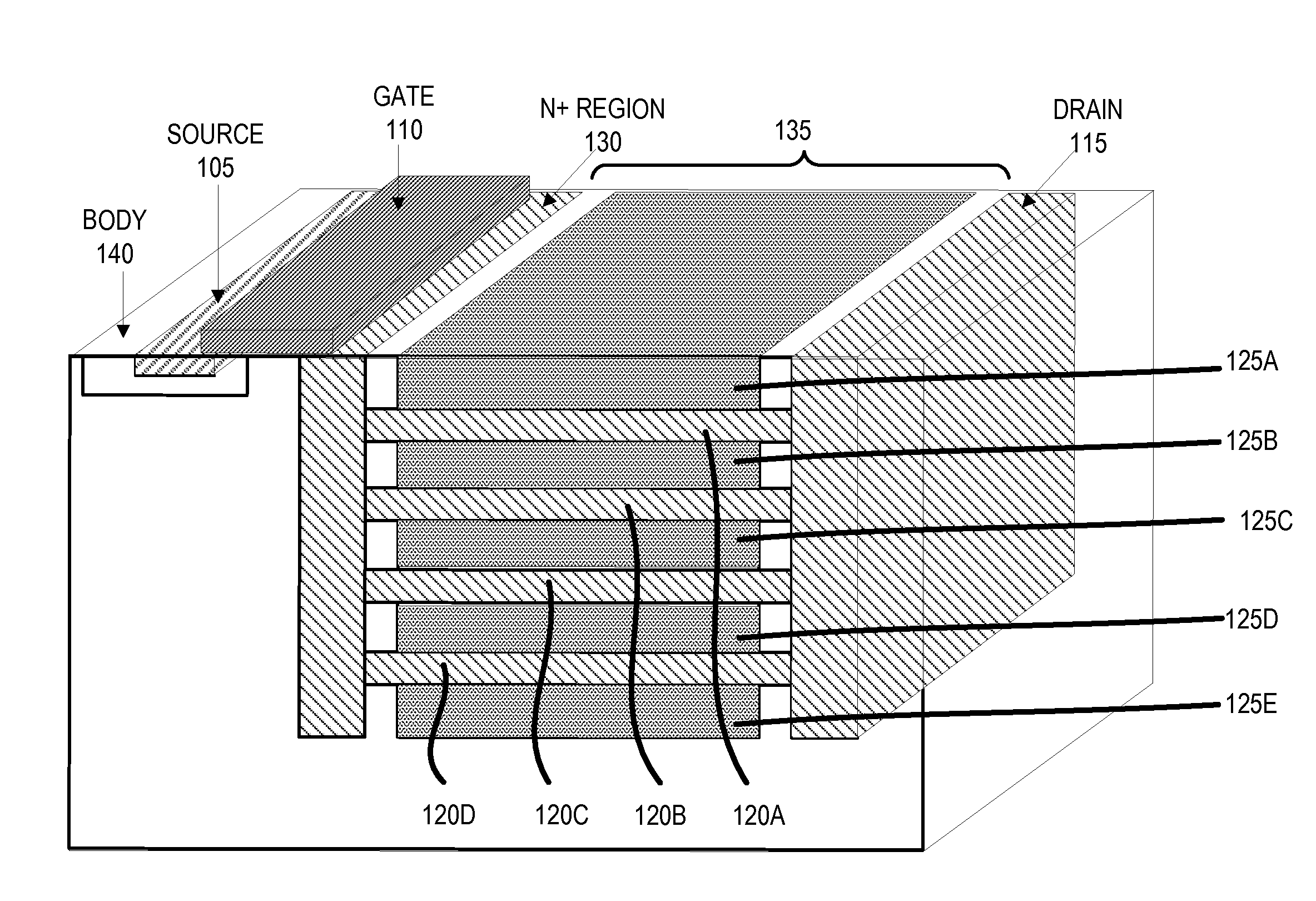
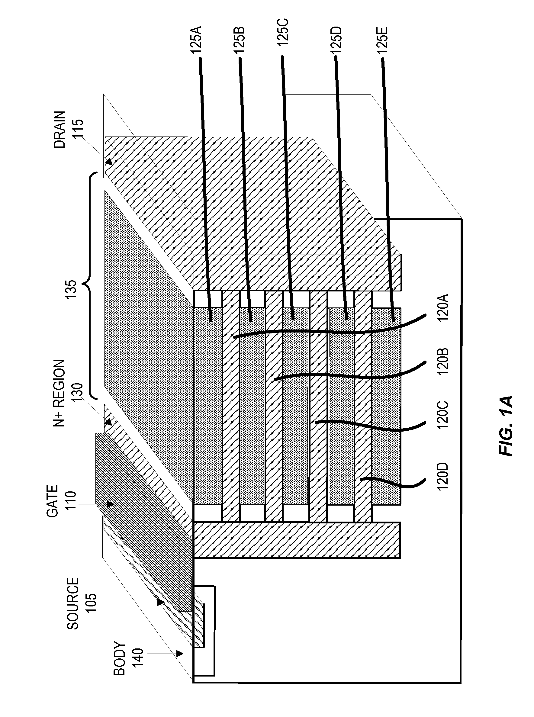
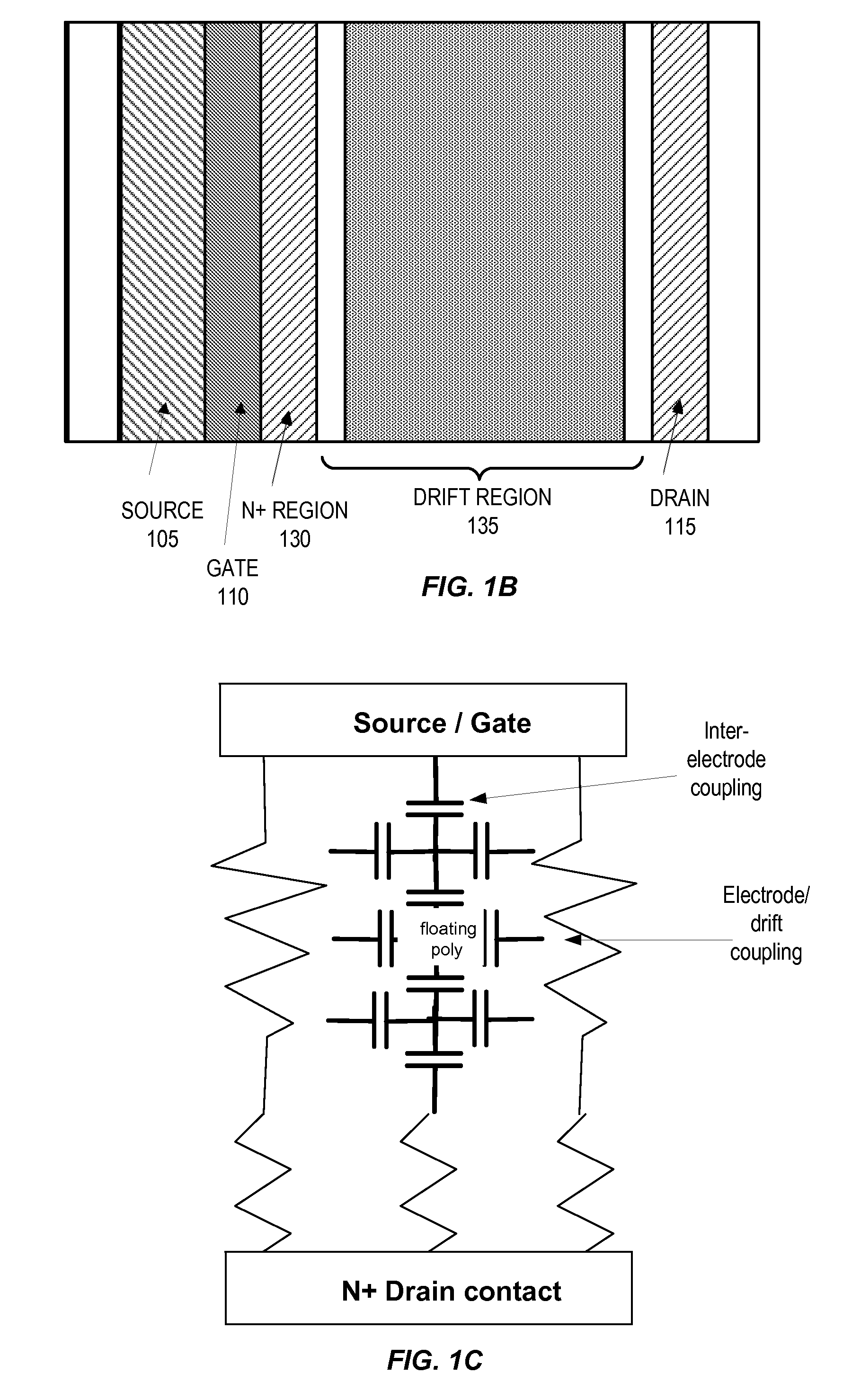
[0060]Embodiments of the present invention provide field effect transistors with lateral floating control capacitors that reduce on-resistance while maintaining higher breakdown voltages. In embodiments, the drift region of a field effect transistor includes an active drift region that conducts current between the source region and the drain region when voltage is applied to the gate region and inactive floating charge control (FCC) regions that field-shape the active drift region to improve breakdown voltage. The inactive FCC regions are vertically stacked in the drift region and are separated by the active drift region. The active drift region can also have a heavily doped portion that is closest to the gate region, and the he...


PUM


Abstract

A semiconductor device includes a source region, a drain region, a gate region, and a drift region. The drift region further includes an active drift region and inactive floating charge control (FCC) regions. The active drift region conducts current between the source region and the drain region when voltage is applied to the gate region. The inactive FCC regions, which field-shape the active drift region to improve breakdown voltage, are vertically stacked in the drift region and are separated by the active drift region. Vertically stacking the inactive FCC regions reduce on-resistance while maintaining higher breakdown voltages.

Description

CROSS-REFERENCE TO RELATED APPLICATIONS[0001]This application claims the benefit of U.S. Provisional Application No. 61 / 124,744, filed Apr. 18, 2008, U.S. Provisional Application No. 61 / 124,786, filed Apr. 18, 2008, U.S. Provisional Application No. 61 / 124,730, filed Apr. 18, 2008, U.S. Provisional Application No. 61 / 124,683, filed Apr. 18, 2008, and U.S. Provisional Application No. 61 / 124,736, filed Apr. 18, 2008, all of which are incorporated herein by reference in their entireties.BACKGROUND OF THE INVENTION[0002]In semiconductor devices, including high voltage devices, it is desirable to obtain a low on-resistance that is primarily determined by the drift region resistance. Typically, the drift region resistance of a transistor is lowered by increasing the doping level of the drift region. However, increasing the doping level of the drift region has the undesirable effect of reducing the breakdown voltage. The doping level of the drift region is therefore optimized to obtain the ...

Claims


Application Information

Patent Timeline
Patent Type & Authority Applications(United States)
IPC IPC(8): H01L27/06
CPCH01L27/0733H01L29/0634H01L29/0653H01L29/7835H01L29/0847H01L29/407H01L29/0692
Inventor YANG, ROBERT KUO-CHANGSHIBIB, MUHAMMED AYMANBLANCHARD, RICHARD A.
Owner SEMICON COMPONENTS IND LLC
Why Eureka
Try Eureka