Semiconductor device

a technology of semiconductor elements and devices, applied in the direction of non-metallic protective coating applications, sustainable manufacturing/processing, final product manufacturing, etc., can solve the problems of failure of connection between semiconductor elements and other devices, operational failures, etc., and achieve high-reliable semiconductors. , the effect of preventing electromigration due to the deposition of wiring metal ions

Active Publication Date: 2005-12-01
SHENZHEN TOREY MICROELECTRONIC TECH CO LTD
View PDF6 Cites 18 Cited by
  • Summary
  • Abstract
  • Description
  • Claims
  • Application Information

AI Technical Summary

Benefits of technology

[0017] The present invention has an objective to provide a high reliable semiconductor device in which electromigration due to deposition of wiring metal ions is prevented.

Problems solved by technology

The connections between the semiconductor element and other devices fail, and operational failures occur.

Method used


Image

  • Semiconductor device
  • Semiconductor device
  • Semiconductor device

Examples


Embodiment Construction

[0059] The present invention addresses electromigration problems in COF (chip on film) and other types of semiconductor devices. Electromigration occurs when the wiring material ionizes and deposits at high humidity. A metal ion binder forming a complex with metal ions is added into a basic component which comes in contact with the wiring. Alternatively, the binder is applied uniformly across the wire surface. The use of the binder restricts metal ion deposition in electromigration. The invention thus provides highly reliable COFs which allow for further reductions in wire pitches and increases in voltage.

[0060] The following will describe an embodiment of the present invention in reference to FIG. 1 through FIG. 8.

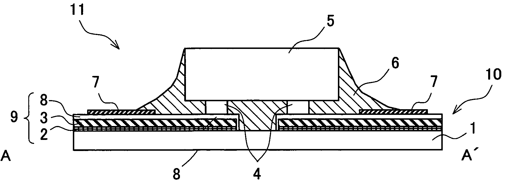
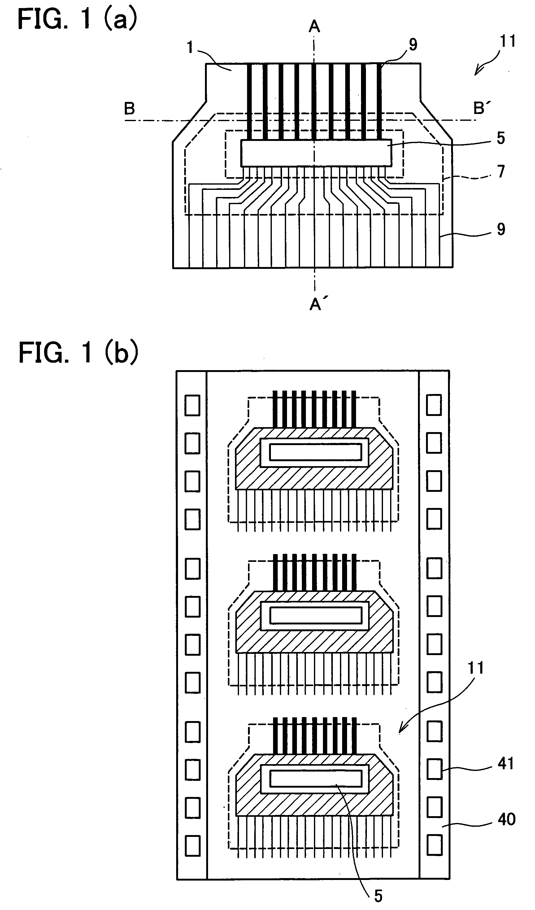
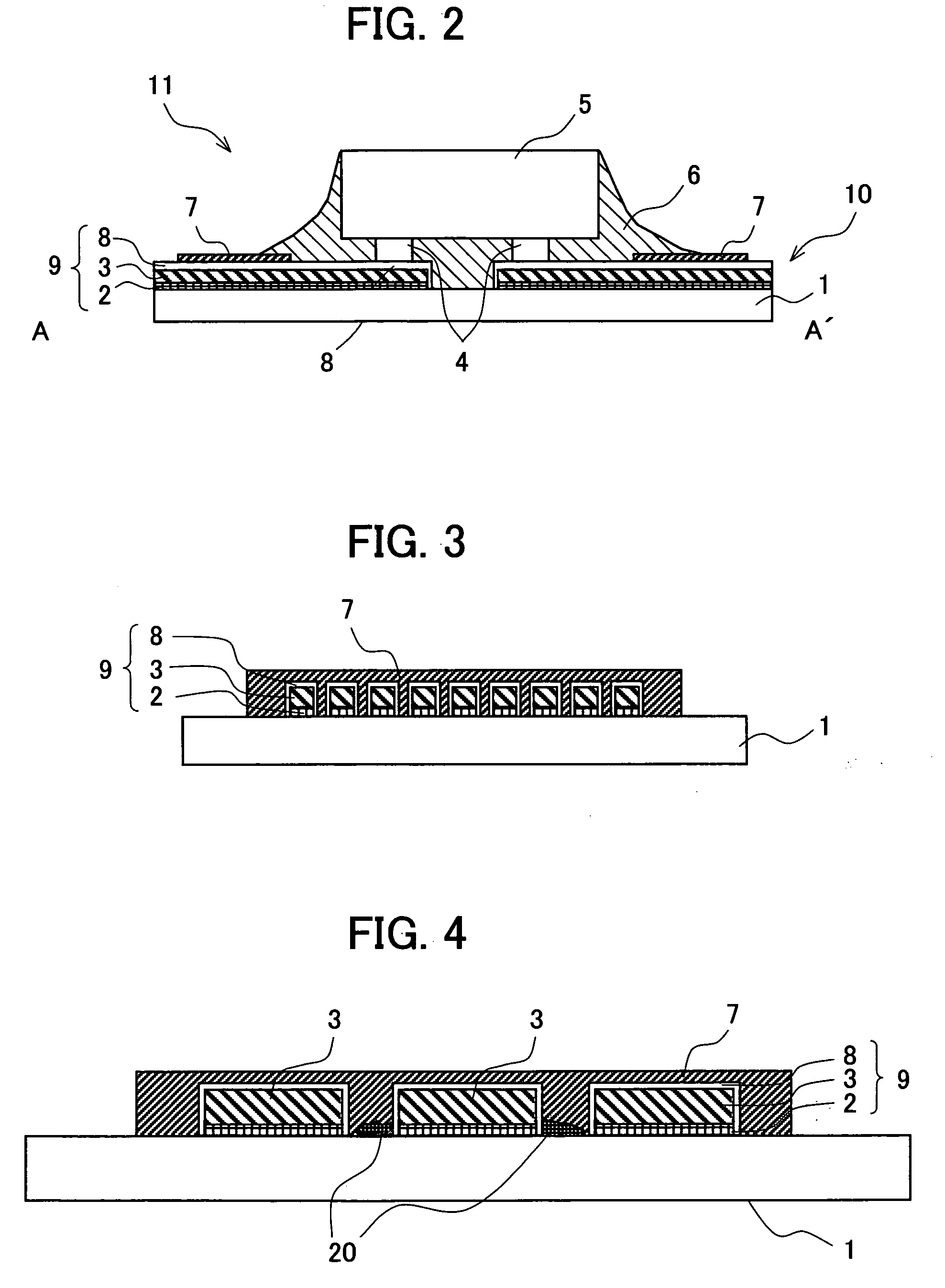
[0061]FIG. 1(a) is a plan view of a semiconductor device in accordance with the present invention. FIG. 2 is a cross-sectional view along line A-A′ in FIG. 1(a). FIG. 3 is a cross-sectional view along line B-B′ in FIG. 1(a).

[0062] A semiconductor device 11 in accordanc...


PUM


Abstract

A high reliability semiconductor device is provided which can prevent electromigration due to the deposition of metal ions originating from wires. The device includes: a flexible wiring board 11 including a base film 1 and multiple wires 9; a semiconductor chip 5 mounted to the flexible wiring board 11; and a sealing resin 6 disposed between the flexible wiring board 11 and the semiconductor chip 5 so as to at least partially in contact with the wires 9. The sealing resin 6 contains a metal ion binder mixed thereto.

Description

[0001] This Nonprovisional application claims priority under 35 U.S.C. § 119(a) on Patent Application No. 2004-152372 filed in Japan on May 21, 2004, the entire contents of which are hereby incorporated by reference. FIELD OF THE INVENTION [0002] The present invention relates in general to semiconductor devices and in particular to those with limited electromigration in wires. BACKGROUND OF THE INVENTION [0003] COFs and TCPs are well-known examples of semiconductor devices carrying electronic components mounted on a wiring board. A COF, or chip on film, contains semiconductor elements mounted / joined onto a flexible wiring board. A TCP, or tape carrier package, contains semiconductor elements continuously joined to a flexible wiring board. The COF and TCP are chiefly applied to semiconductor devices containing a LCD (liquid crystal driver) IC. [0004] Recent demand for LCDs with increased numbers of outputs is rapidly pushing the flexible wiring board for LCD ICs to finer wiring patte...

Claims


Application Information

Patent Timeline
Patent Type & Authority Applications(United States)
IPC IPC(8): H01L23/29H01L21/56H01L21/60H01L23/12H01L23/14H01L23/31H01L23/48H01L23/498H05K1/00H05K3/28H05K3/30
CPCH01L21/563H01L23/145H01L2924/01322H01L2224/32225H05K2203/124H01L23/4985H01L23/49883H01L23/49894H01L2224/16225H01L2224/73203H01L2224/73204H01L2924/01078H01L2924/01079H05K1/0393H05K3/285H05K3/305H05K2201/0769H05K2201/10674H05K2201/10977H05K2203/122H01L2924/00Y02P70/50H01L23/28
Inventor FUKUTA, KAZUHIKOTOYOSAWA, KENJIKIDOGUCHI, TAKASHI
Owner SHENZHEN TOREY MICROELECTRONIC TECH CO LTD
Why Eureka
Try Eureka