Semiconductor device

Active Publication Date: 2008-12-04
ROHM CO LTD
View PDF8 Cites 9 Cited by
  • Summary
  • Abstract
  • Description
  • Claims
  • Application Information

AI Technical Summary

Benefits of technology

[0024]In this arrangement, the titanium nitride film is the portion of the barrier layer that contacts the tungsten plug. Thus even when the tungsten plug is formed by a CVD method using tungsten hexaf luoride gas (WF6 gas), the WF6 gas can be prevented from diffusing into the insulating film and corroding the insulating film.
[0025]In addition, because the tungsten plug contacts the titanium nitride film that is excellent in adhesion with tungsten, adhesion of the barrier layer and the tungsten plug can be improved. Meanwhile, because the copper wire contacts the tantalum film

Problems solved by technology

However, because Cu has a property of corroding due to oxidation, when the portion of the second Cu wire is left exposed from the penetrating hole, the exposed portion of the second Cu wire becomes corroded and reliability of electrical connection with the external portion may degrade.
In order to form the electrode pad made of Al, after forming the second Cu wire in

Method used


Image

  • Semiconductor device
  • Semiconductor device
  • Semiconductor device

Examples


first embodiment

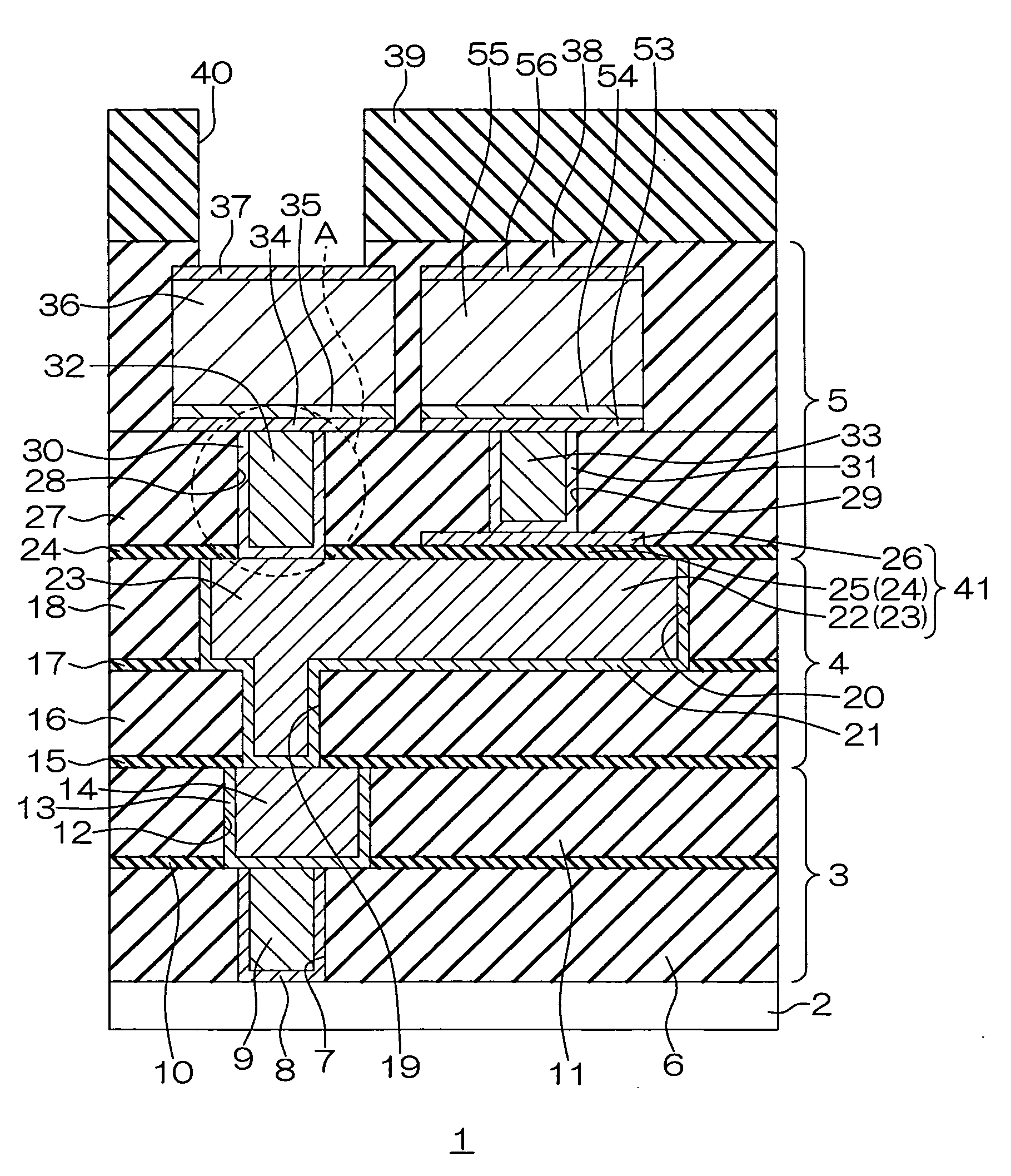
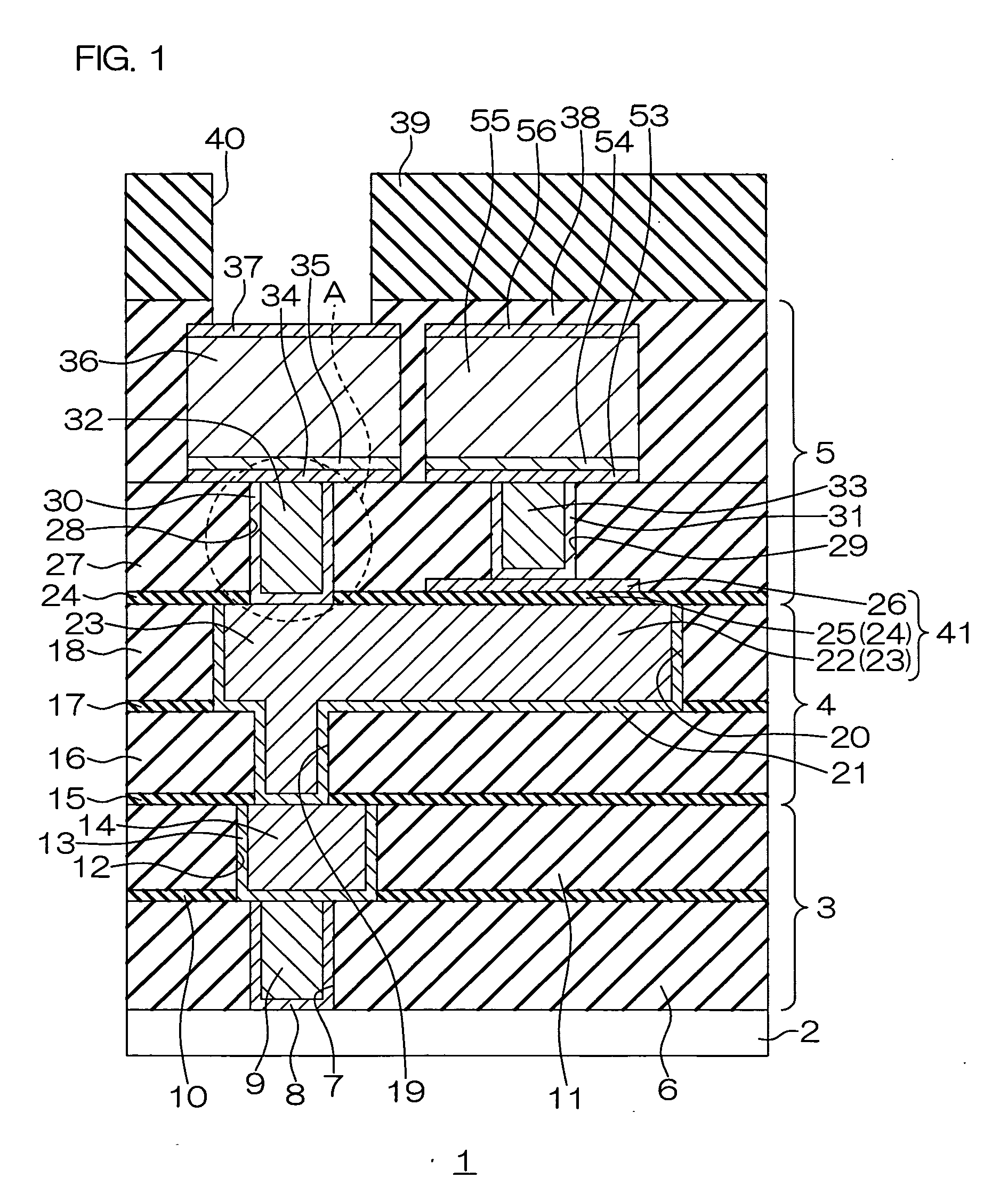
[0050]FIG. 1 is a schematic sectional view showing an arrangement of a semiconductor device according to the present invention.

[0051]On a semiconductor substrate 2 formed of Si (silicon), for example, the semiconductor device 1 has a multilayer wiring structure having a first wiring layer 3, a second wiring layer 4, and a third wiring layer 5 laminated in that order starting from the semiconductor substrate 2 side.

[0052]A functional device (not shown), such as MOSFET (metal oxide semiconductor field effect transistor), is built on a surface layer portion of the semiconductor substrate 2.

[0053]The first wiring layer 3 includes an interlayer film 6 formed of SiO2 (silicon oxide) and laminated on the semiconductor substrate 2, a diffusion preventing film 10 formed of SiC (silicon carbide) laminated on the interlayer film 6, and an interlayer film 11 formed of SiO2 and laminated on the diffusion preventing film 10.

[0054]In the interlayer film 11 and the diffusion preventing film 10 a wi...

second embodiment

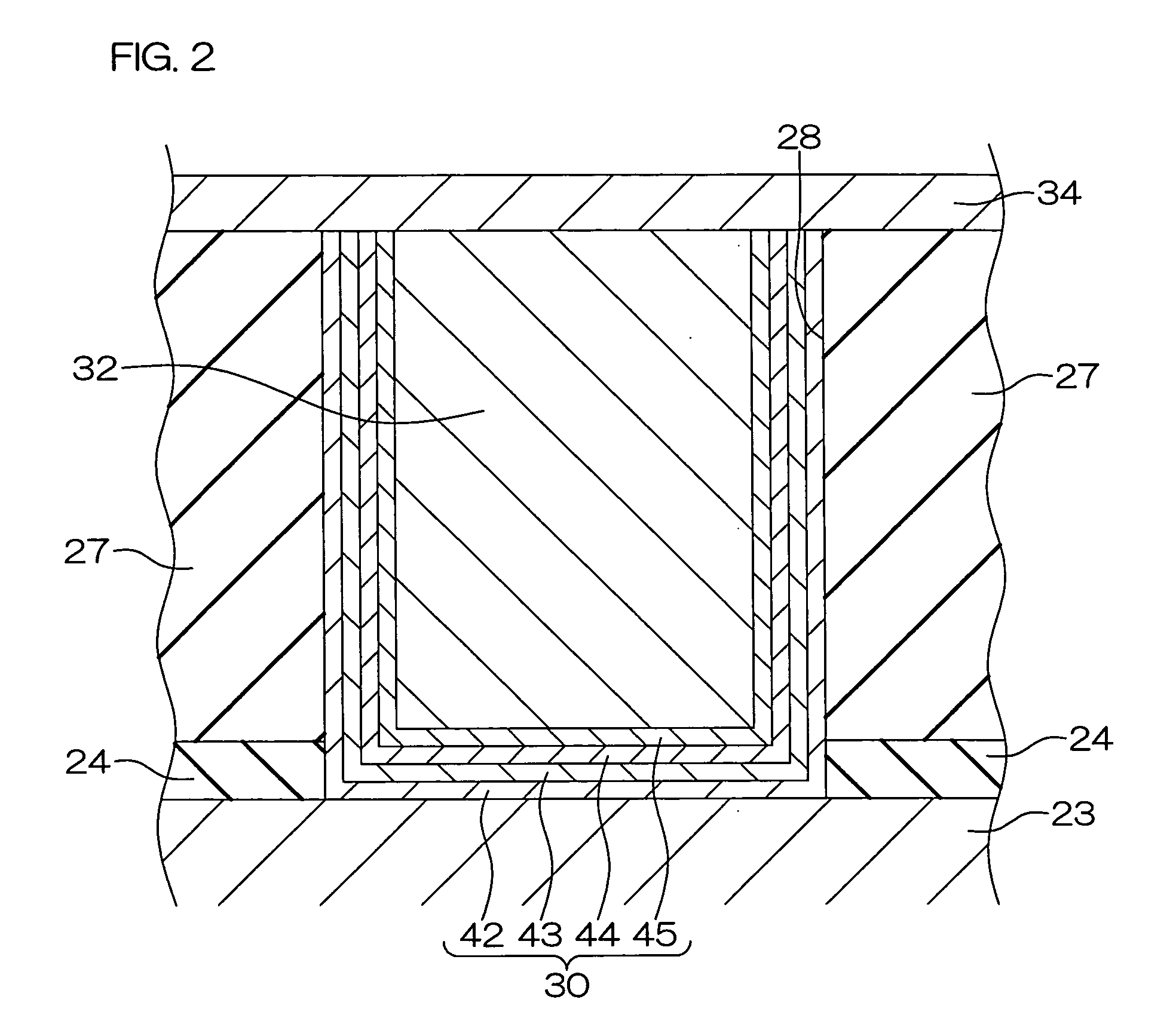
[0118]FIG. 4 is a schematic sectional view showing an arrangement of a semiconductor device 47 according to the present invention. In FIG. 4, portions corresponding to portions shown in FIG. 1 are provided with the same reference symbols as those of FIG. 1.

[0119]In the arrangement shown in FIG. 4, the semiconductor device 47 is a semiconductor device to which a WL-CSP (wafer level-chip size package) technique is applied.

[0120]In the semiconductor device 47, a penetrating hole 46 reaching the aluminum wire 36 is formed in the interlayer film 38. A portion of the aluminum wire 36 facing the penetrating hole 46 is exposed via the penetrating hole 46. An aluminum rewire 48 is connected to the aluminum wire 36, having aluminum as a main component and drawn out on the surface of the interlayer film 38 via the penetrating hole 46. A portion of the aluminum rewire 48 drawn out on the surface of the interlayer film 38 is coated with a surface protective film 49 formed of SiN.

[0121]A protecti...


PUM


Abstract

A semiconductor device according to the present invention has a multilayer wiring structure laminating and disposing a plurality of with sandwiching an insulating film and includes: a copper wire having copper as a main component; an insulating film formed on the copper wire; an aluminum wire having aluminum as a main component and formed on the insulating film to be electrically connected to the copper wire via a via hole formed to penetrate through the insulating film; and a surface protective film formed on the aluminum wire; and the surface protective film formed with a pad opening exposing a portion of the aluminum wire as an electrode pad for electrical connection with an external portion.

Description

BACKGROUND OF THE INVENTION[0001]1. Field of the Invention[0002]The present invention relates to a semiconductor device with a multilayer wiring structure.[0003]2. Description of Related Art[0004]A so-called multilayer wiring structure, in which a plurality of wiring layers are laminated on a semiconductor substrate, is employed in a semiconductor device, such as an LSI of a high integration.[0005]In semiconductor devices employing such a multilayer wiring structure, in place of Al (aluminum) which has been conventionally used as a wiring material, application of Cu (copper), which is higher in conductivity is being studied in order to reduce wiring resistance.[0006]In a multilayer wiring structure using a Cu wiring material, a first insulating film formed of SiO2 (silicon oxide) is laminated onto a semiconductor substrate formed of Si (silicon). A microscopic wiring groove corresponding to a predetermined wiring pattern is formed in a surface layer portion of the first insulating f...

Claims


Application Information

Patent Timeline
IPC IPC(8): H01L29/92H01L23/52
CPCH01L23/5223H01L23/53223H01L2224/05647H01L2224/05184H01L2224/05181H01L2224/05166H01L2224/05001H01L2224/05548H01L2224/05026H01L23/53238H01L23/53295H01L27/0805H01L28/60H01L2224/13H01L2924/13091H01L2924/00H01L2924/00014H01L24/05
Inventor NAKAO, YUICHIYAMAHA, TAKAHISA
Owner ROHM CO LTD
Why Eureka
Try Eureka