Nanotube-based switching elements with multiple controls

a technology of switching elements and nanotubes, applied in the field of nanotube switching circuits, can solve the problems of high power consumption, density and operation speed of mos digital circuits, and limited density of bipolar digital integrated circuits

Active Publication Date: 2005-12-08
NANTERO
View PDF80 Cites 45 Cited by
  • Summary
  • Abstract
  • Description
  • Claims
  • Application Information

AI Technical Summary

Problems solved by technology

However, the density of bipolar digital integrated circuits is limited by their high power consumption and the ability of packaging technology to dissipate the heat produced while the circuits are operating.
The density and operating speed of MOS digital circuits are still limited by the need to dissipate the heat produced when the device is operating.
Digital logic integrated circuits constructed from bipolar or MOS devices do not function correctly under conditions of high heat or extreme environments.
As leakage current increases, the operating temperature of the device rises, the power consumed by the circuit increases, and the difficulty of discriminating the off state from the on state reduces circuit reliability.
Conventional digital logic circuits also short internally when subjected to certain extreme environments because electrical currents are generated inside the semiconductor material.
It is possible to manufacture integrated circuits with special devices and isolation techniques so that they remain operational when exposed to such environments, but the high cost of these devices limits their availability and practicality.
In addition, such digital circuits exhibit timing differences from their normal counterparts, requiring additional design verification to add protection to an existing design.
Integrated circuits constructed from either bipolar or FET switching elements are volatile.
Alternative solutions to avoid losing information in volatile digital circuits, such as battery backup, also add cost and complexity to digital designs.

Method used


Image

  • Nanotube-based switching elements with multiple controls
  • Nanotube-based switching elements with multiple controls
  • Nanotube-based switching elements with multiple controls

Examples


Embodiment Construction

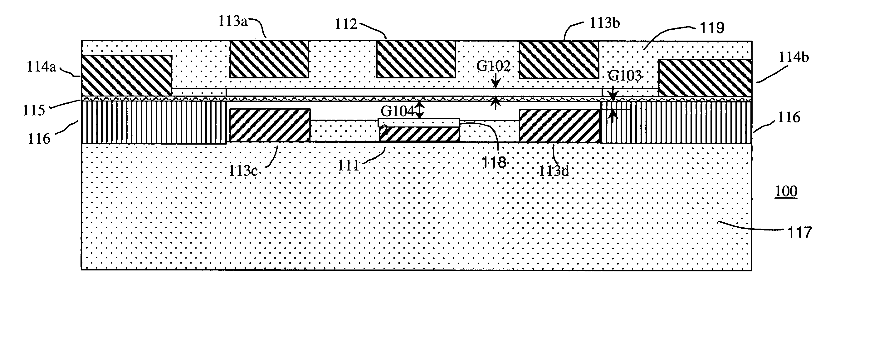
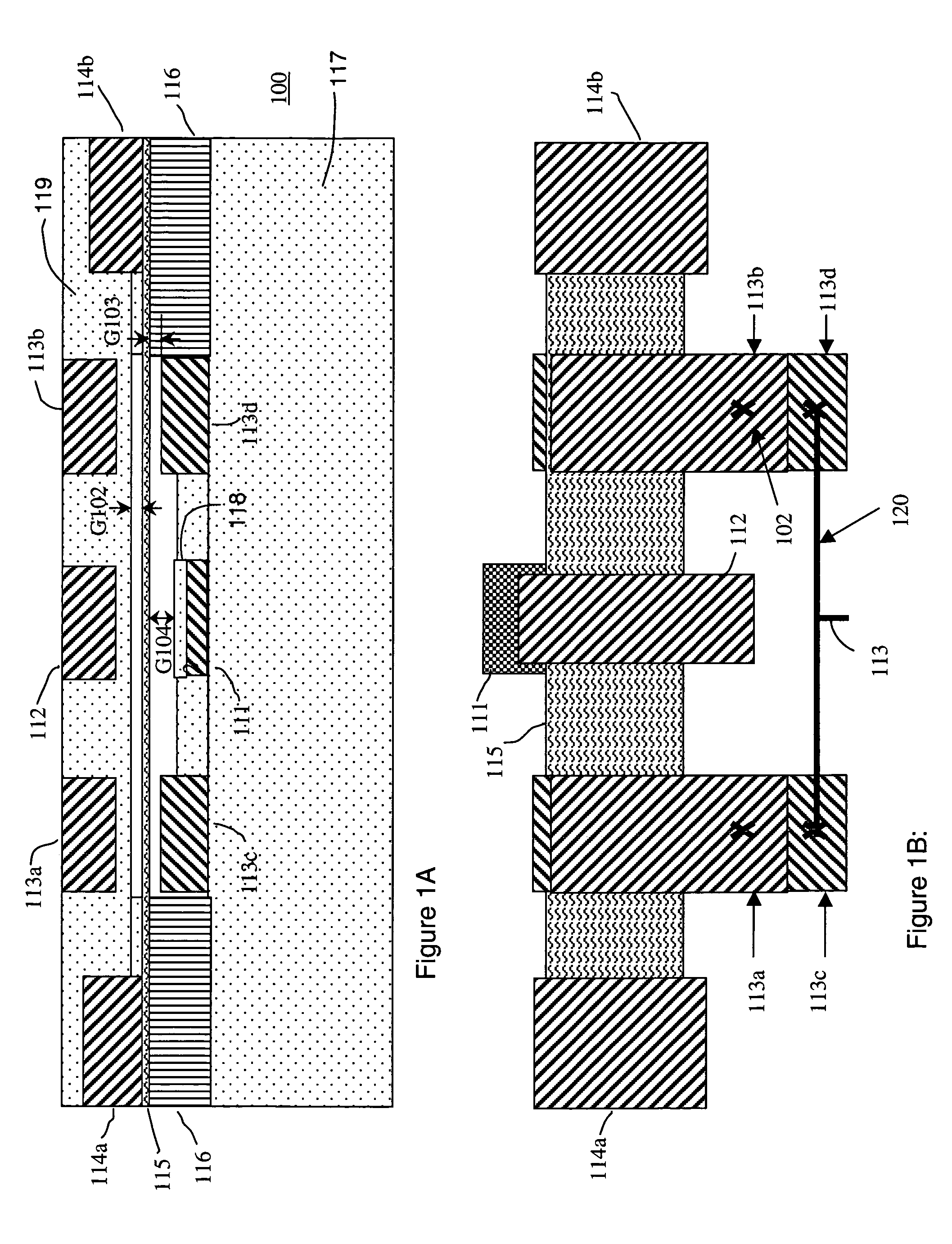
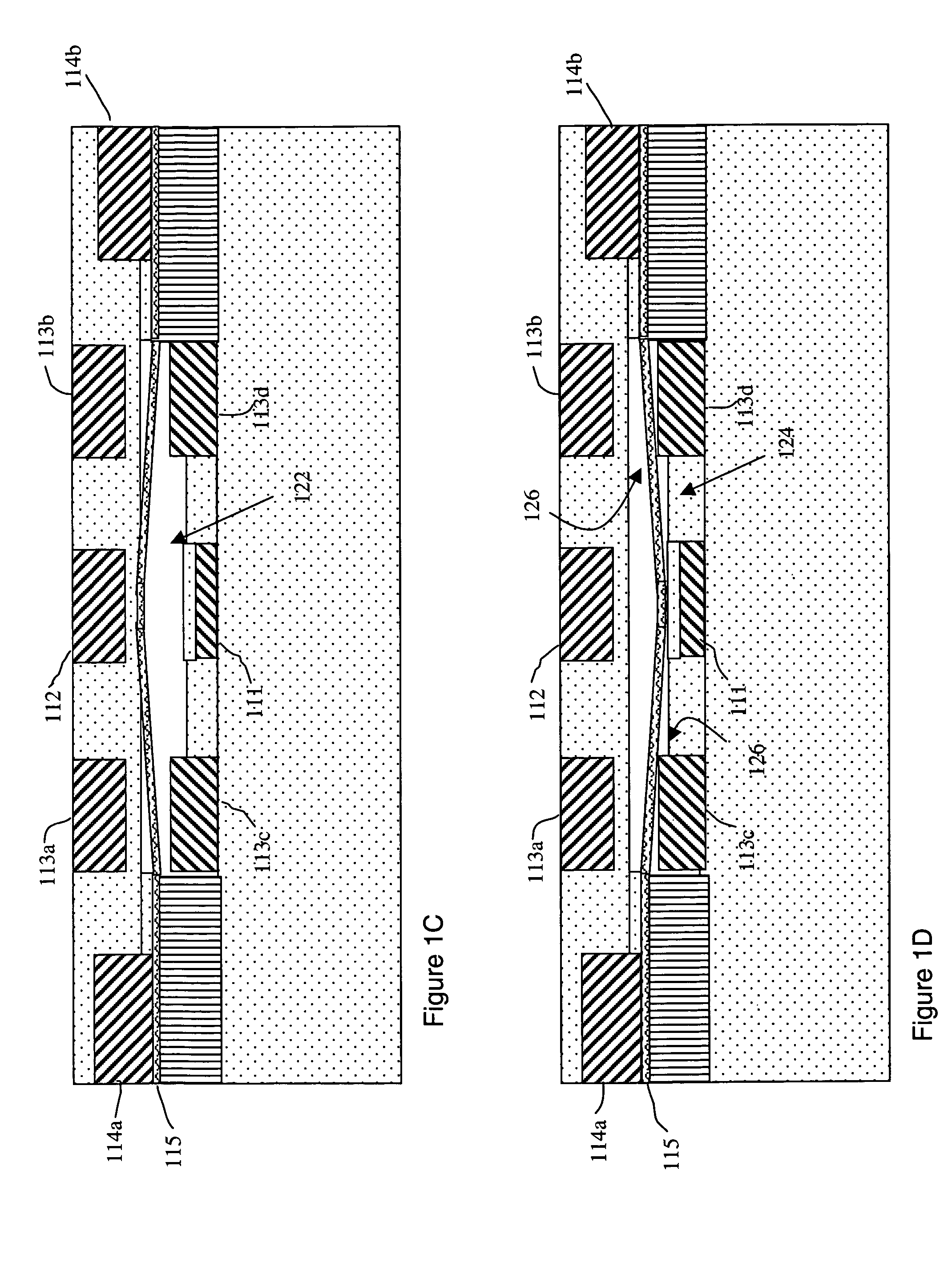
[0037] Preferred embodiments of the invention provide switching elements in which a nanotube-based channel may be controllably formed and unformed, so that a signal may be transferred from a signal node to an output node. The switching element includes multiple control electrodes to control the formation and unformation of the channel, to provide a dual-rail capability, and to be used in novel ways. The transferred signal may be a varying signal or a reference signal, depending on the manner in which the switching element is utilized and arranged. Preferred embodiments provide an isolation structure so that such signal transfer and the switching element's operation is substantially invariant to the output state. For example, the output node may float and / or be tied to other electrical components and the circuit will operate in a predictable switch-like manner. Consequently, the switching elements may be formed into larger circuits, such as Boolean logic circuits. Under some embodime...


PUM


Abstract

Nanotube-based switching elements with multiple controls and circuits made from such. A switching element includes an input node, an output node, and a nanotube channel element having at least one electrically conductive nanotube. A control structure is disposed in relation to the nanotube channel element to controllably form and unform an electrically conductive channel between said input node and said output node. The output node is constructed and arranged so that channel formation is substantially unaffected by the electrical state of the output node. The control structure includes a control electrode and a release electrode, disposed on opposite sides of the nanotube channel element. The control and release may be used to form a differential input, or if the device is constructed appropriately to operate the circuit in a non-volatile manner. The switching elements may be arranged into logic circuits and latches having differential inputs and / or non-volatile behavior depending on the construction.

Description

CROSS-REFERENCE TO RELATED APPLICATIONS [0001] This application is a continuation of and claims priority under 35 U.S.C. §120 to U.S. patent application Ser. No. 10 / 918,085, filed on Aug. 13, 2004, entitled Nanotube-Based Switching Elements with Multiple Controls which claims priority under 35 U.S.C. § 119(e) to U.S. Provisional Patent Application No. 60 / 494,889, filed on Aug. 13, 2003, entitled Nanoelectromechanical Nanotube-Based Logic, which is incorporated herein by reference in its entirety. This application also claims priority under 35 U.S.C. § 119(e) to U.S. Provisional Patent Application No. 60 / 561,330, filed on Apr. 12, 2004, entitled Non-volatile CNT Dual-Rail Differential Logic, which is incorporated herein by reference in its entirety. [0002] This application is related to the following references: [0003] U.S. patent application Ser. No. 10 / 917,794, filed on Aug. 13, 2004, entitled Nanotube-Based Switching Elements; [0004] U.S. patent application Ser. No. 10 / 917,893, fi...

Claims


Application Information

Patent Timeline
Patent Type & Authority Applications(United States)
IPC IPC(8): G11C11/00G11C11/21G11C11/50G11C13/02G11C23/00H01H1/027H01H59/00H01L21/00H01L27/28H01L29/06H01L29/73H01L29/772H01L29/78H01L51/30
CPCB82Y10/00G11C13/025G11C23/00G11C2213/17H01H1/0094H01H1/027H01L27/28H01L29/0665H01L29/0673H01L29/73H01L29/78H01L51/0048H01L51/0508Y10S977/932Y10S977/936Y10S977/943Y10S977/938Y10S977/708Y10S977/94H10K85/221H10K10/46H10K19/80H10K19/00
Inventor BERTIN, CLAUDE L.RUECKES, THOMASSEGAL, BRENT M.
Owner NANTERO
Why Eureka
Try Eureka