Nanofluidic channels with integrated charge sensors and methods based thereon

a technology of charge sensor and nanowire, applied in the field of nanowire, can solve the problems of affecting the optical length detection measurement, difficult to functionalize certain types of nanowire at all, and shifting of nanowire conductivity,

Active Publication Date: 2011-09-22
CORNELL UNIVERSITY
View PDF36 Cites 184 Cited by
  • Summary
  • Abstract
  • Description
  • Claims
  • Application Information

AI Technical Summary

Problems solved by technology

One of the key challenges in utilizing nanowires for detection, therefore, has been to force a molecule to be a distance from the nanowire that is roughly equal to, or less than, the ionic screening length.
If adhesion to the surface occurs, the target molecule is often within the screening length and may cause a shift in nanowire conductivity through the electric field effect.
There are disadvantages to this, including but not limited to the fact that a nanowire may need to be functionalized with a specific chemical for each target molecule, or that it is difficult to functionalize certain types of nanowires at all.
There are several physical limitations to optical length detection measurements.
In its standard state, this equipment often consumes the space on an entire optical table and much of it cannot be miniaturized, even in its most advanced and costly form.
This severely limits product designers who would like to make portable, and low cost “lab-on-chip” devices.
Second, the spatial resolution provided by optical systems is limited.
Owing to the wave nature of light and the typical wavelengths used in fluorescent microscopy, the spatial resolution available using even the best optical systems is limited to around 200 nm.

Method used


Image

  • Nanofluidic channels with integrated charge sensors and methods based thereon
  • Nanofluidic channels with integrated charge sensors and methods based thereon
  • Nanofluidic channels with integrated charge sensors and methods based thereon

Examples


example 1

6.1 Example 1

Nanofluidic Channels with Integrated Carbon Nanotube Charge Sensors

6.1.1 Introduction

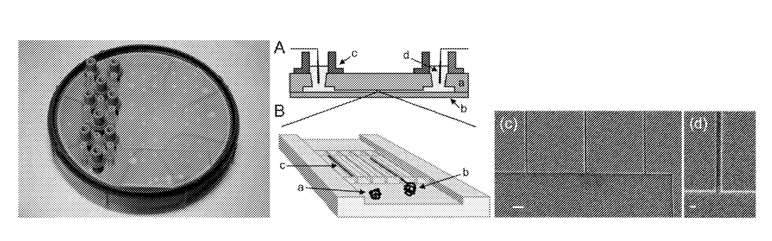
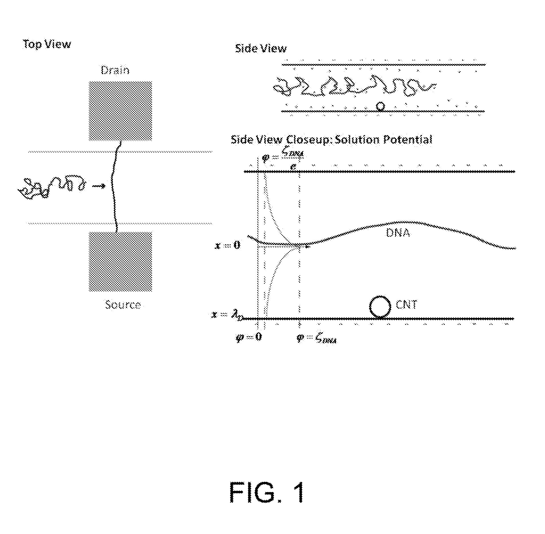
[0319]This example demonstrates that a electrical detector comprising a nanofluidic channel and a carbon nanotube sensor integrated in the nanofluidic channel can be used as means for electronically detecting charged molecules in a highly confined environment while allowing for simultaneous fluorescent observation. Subsequent Examples (Sections 6.2-6.4) describe methods for fabricating electrical detectors comprising a nanofluidic channel and a charge sensor integrated in the nanofluidic channel, wherein the charge sensor is a nanowire or nanotube.

[0320]Individually addressable, semiconducting, single-walled carbon nanotubes were incorporated into fluid-filled channels with depths of 15-100 nm and widths of 500 nm. Given appropriate buffer conditions, channels of this size are comparable in depth to the length scale of ionic screening. Thus, charged DNA molecules travelling through the ...

example 2

6.2 Example 2

Fabrication of Device Comprising a Nanofluidic Channel with an Integrated Carbon Nanotube

6.2.1 Introduction

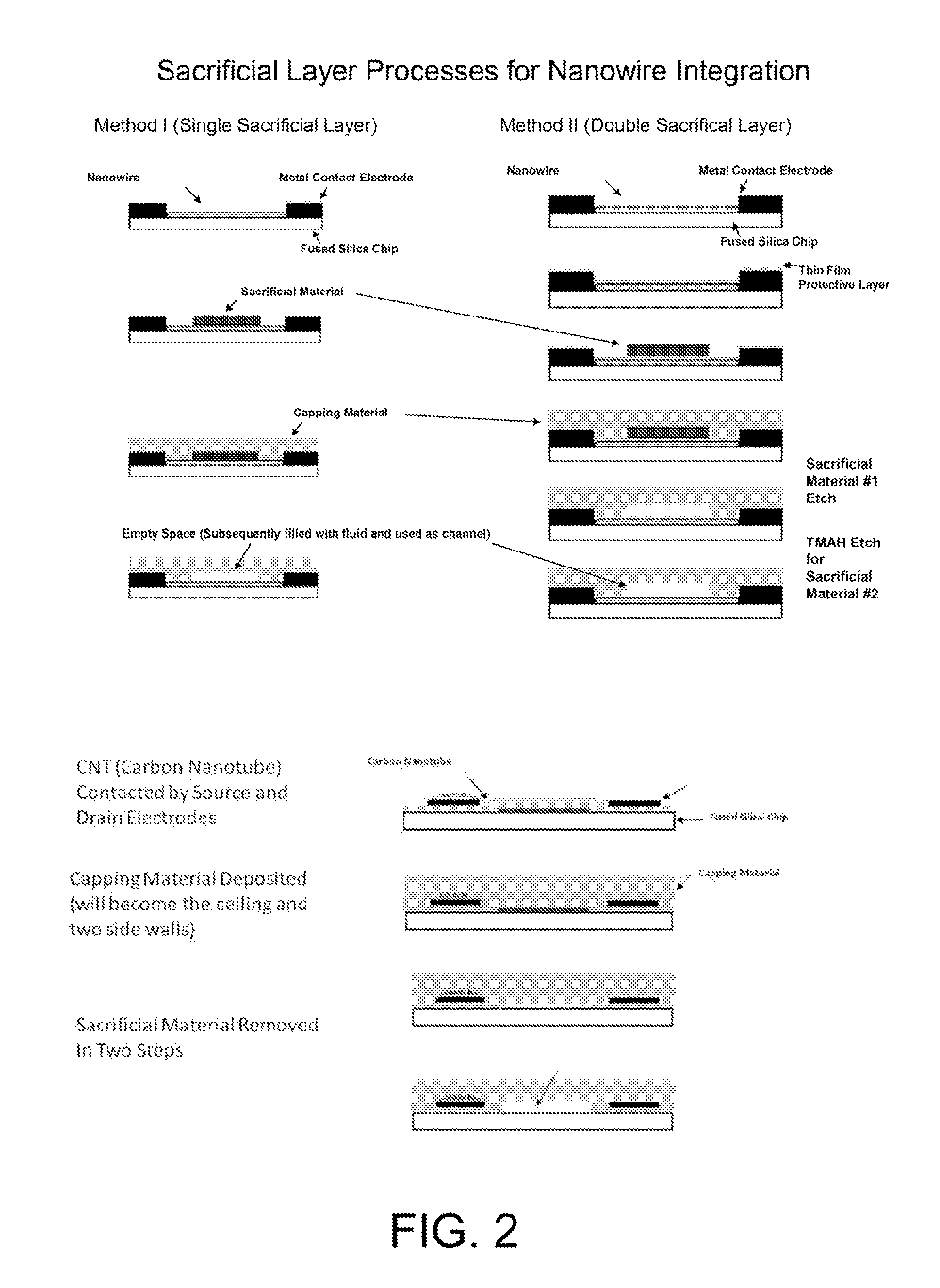
[0381]The electrical detector described in Section 6.1 was fabricated by a method that comprised a combination of standard micro-electro-mechanical (MEMS) processing techniques known in the art, as well as carbon nanotube growth techniques well known in the art. This example describes a preferred embodiment for a method for producing nanofluidic channel devices with integrated carbon nanotube sensors.

[0382]Section 6.3 sets forth a specific embodiment of the fabrication method.

6.2.2 Device Characteristics

[0383]Based on the concepts for electrical detection of charged DNA molecules in nanofluidic channels using integrated carbon nanotubes outlined in Section 6.1, an electrical detector comprising a nanofluidic channel and a charge sensor integrated in the nanofluidic channel preferably has the following characteristics:

[0384](1) Nanofluidic channel depths are prefera...

example 3

6.3 Example 3

Detailed Protocol for Fabrication of Device Comprising a Nanofluidic Channel with an Integrated Carbon Nanotube

[0508]The following is an example of a fabrication protocol that has been carried out based on the methods for fabricating the electrical detector set forth in Section 6.2 (Example 2).

[0509]Step 1: Fabrication of Alignment Layer[0510]1. Pre-Processing:[0511]a. Obtain three, 100 mm diameter, 170 μm thick, fused silica wafers. (Mark Optics) Wafers should have a scratch dig parameter of 40 / 20 or lower, and an RMS surface roughness of [0512]b. Scribe Wafer Numbers onto back of wafers using a diamond scribe.[0513]c. Clean wafers in an automated spin-rinse-dry machine.[0514]2. Photoresist Preparation:[0515]a. p-20 primer; spin at 3000 RPM, 5000 R / S, 45 sec[0516]b. SPR 220 3.0 Photoresist; spin at 3000 RPM, 5000 R / S, 45 sec[0517]c. Bake on hotplate at 115° C. for 2 min.[0518]3. Photolithography in Autostep Mask Aligner[0519]a. Load the desired photolithography mask in...


PUM

PropertyMeasurementUnit
depthaaaaaaaaaa
radius of gyrationaaaaaaaaaa

Abstract

An electrical detector is provided that comprises a nanofluidic channel with an integrated nanoscale charge sensor. The charge sensor can be an unfunctionalized nanowire, nanotube, transistor or capacitor and can be of carbon, silicon, carbon / silicon or other semiconducting material. The nanofluidic channel depth is on the order of the Debye screening length. Methods are also provided for detecting charged molecules or biological or chemical species with the electrical detector. Charged molecules or species in solution are driven through the nanofluidic channel of the electrical detector and contact the charge sensor, thereby producing a detectable signal. Methods are also provided for detecting a local solution potential of interest. A solution flowing through the nanofluidic channel of the electrical detector contacts the charge sensor, thereby producing a detectable local solution potential signal.

Description

CROSS-REFERENCE TO RELATED APPLICATIONS [0001]This application claims priority to and the benefit of co-pending U.S. provisional patent application Ser. No. 61 / 080,170, entitled “Nanofluidic Channels with Integrated Nanowires,” filed Jul. 11, 2008, which is incorporated herein by reference in its entirety.STATEMENT REGARDING FEDERALLY SPONSORED RESEARCH OR DEVELOPMENT[0002]The disclosed invention was made with government support under contract no. NSF 9876771 from the National Science Foundation, NIH HG001506 from the National Institutes of Health, and agreement no. ECS-9876771 from the STC Program of the National Science Foundation. The government has rights in this invention.1. TECHNICAL FIELD[0003]The present invention relates to nanofluidic channels (“nanochannels”) with integrated charge sensors such as nanotuhes, nanowires, transistors or capacitors. The invention also relates to methods for detecting biological or chemical species in nanofluidic channels with charge sensors. ...

Claims


Application Information

Patent Timeline
Patent Type & Authority Applications(United States)
IPC IPC(8): H01L29/66G01N27/00H01J49/00
CPCB01L3/502761B01L2300/0896G01N33/48721G01N27/414G01N27/4473B82Y30/00
Inventor MANNION, JOHN T.CRAIGHEAD, HAROLD C.
Owner CORNELL UNIVERSITY
Why Eureka
Try Eureka