Self-aligned nanotube field effect transistor and method of fabricating same

a field effect transistor and self-aligning technology, applied in the field of carbon-nanotube field effect transistors, can solve the problems of no known system or method that implements a nanotube, the capacitance of a carbon-nanotube transistor does not scale inversely, and the difficulty of further reduction

Inactive Publication Date: 2005-05-10
GLOBALFOUNDRIES U S INC
View PDF12 Cites 181 Cited by
  • Summary
  • Abstract
  • Description
  • Claims
  • Application Information

AI Technical Summary

Problems solved by technology

Significantly, further reduction can be difficult to achieve since gate leakage through the dielectric film increases exponentially for an oxide thickness below 4 nm.
However, the gate capacitance for a carbon-nanotube transistor does not scale inversely proportional with the dielectric film thickness.
No known system or method has implemented a nanotube to achieve performance and smaller size in an FET.

Method used


Image

  • Self-aligned nanotube field effect transistor and method of fabricating same
  • Self-aligned nanotube field effect transistor and method of fabricating same
  • Self-aligned nanotube field effect transistor and method of fabricating same

Examples


Embodiment Construction

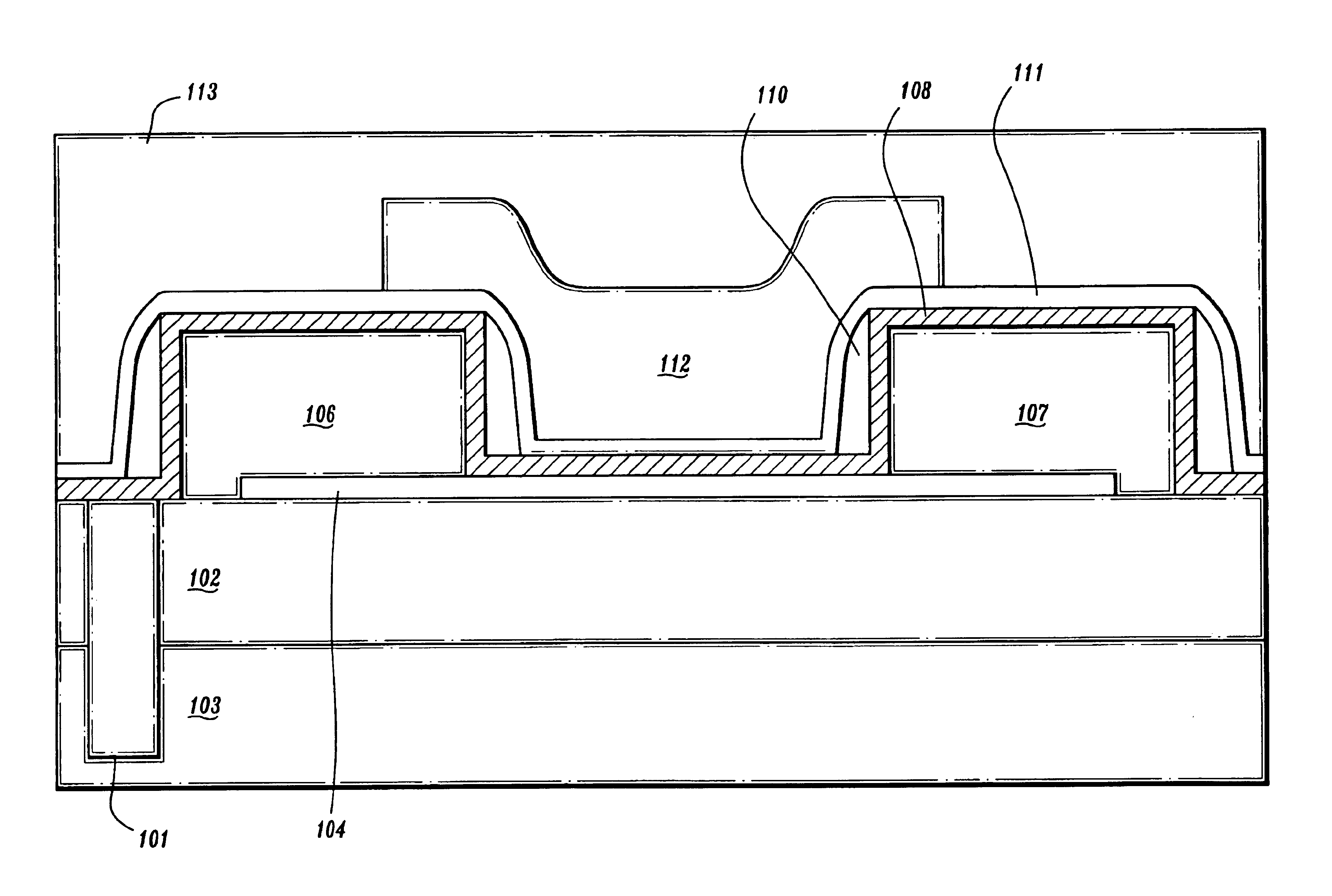
[0033]According to an embodiment of the present invention, a gate, a source and a drain of a field effect transistor (FET) are self-aligned, thereby reducing overlap capacitances.

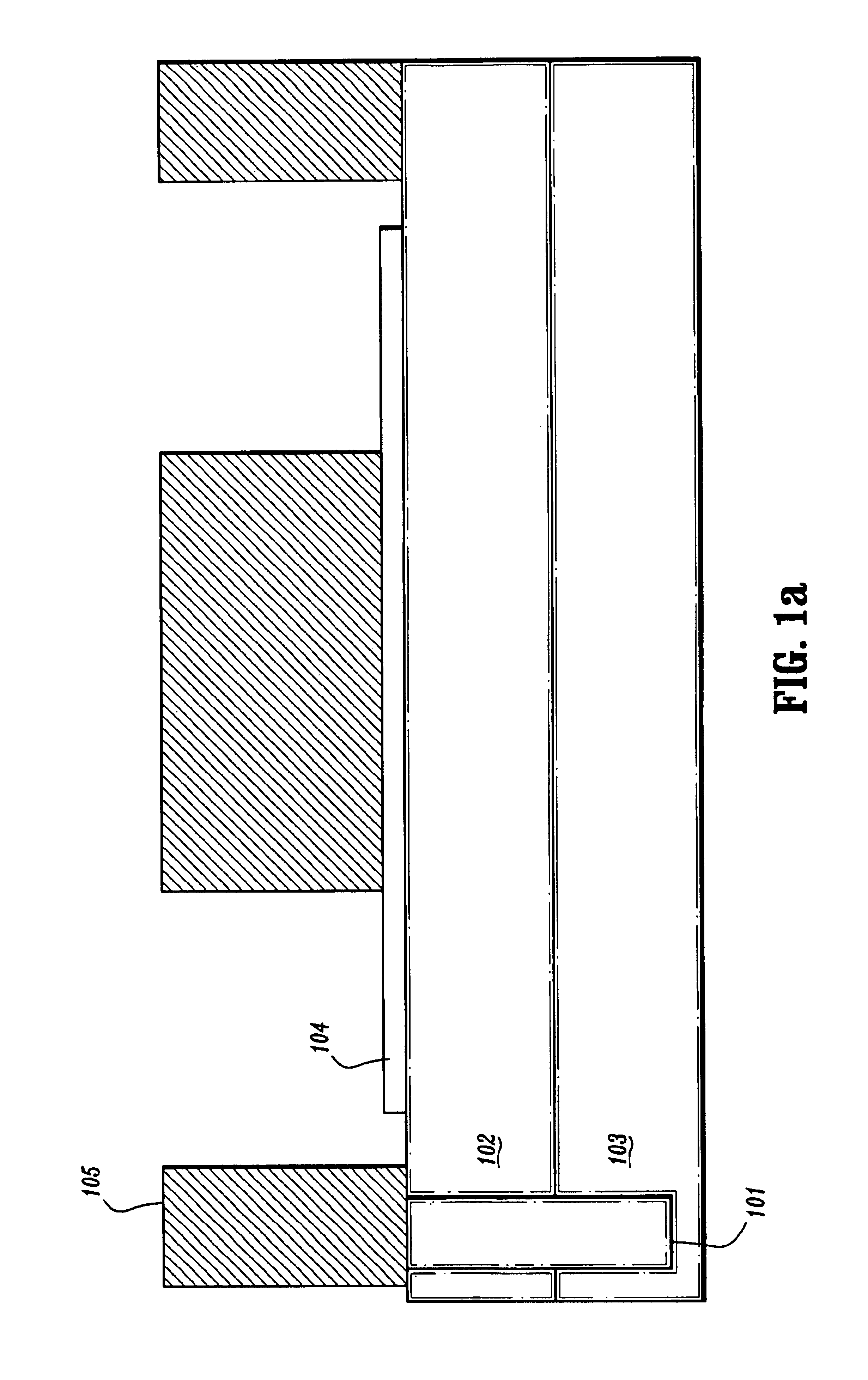
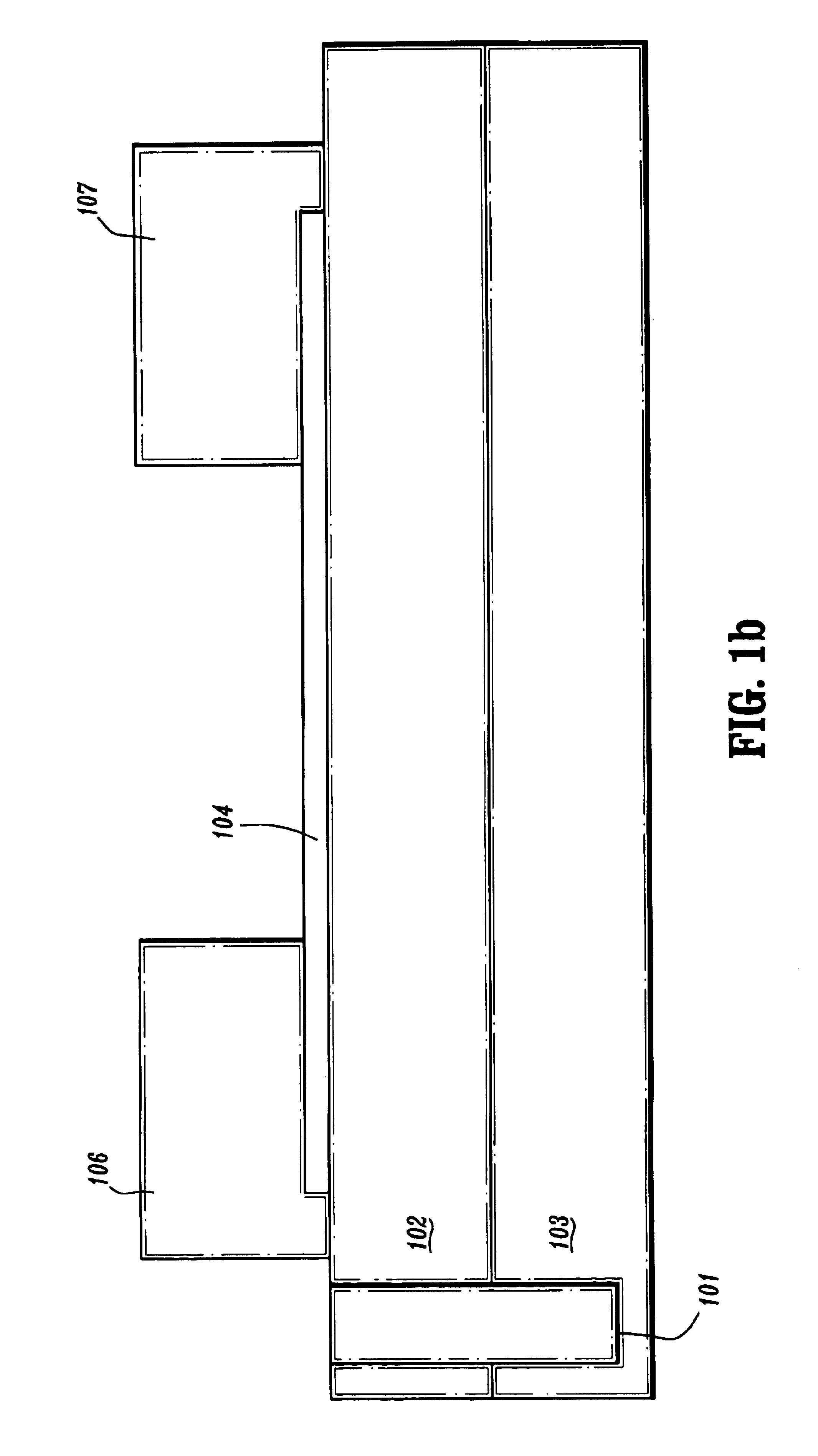
[0034]According to an embodiment of the present invention, a carbon-nanotube FET can be fabricated using a pattern transfer by lift-off etch, wherein the source and the drain are formed before the gate. Referring to FIGS. 1a-i, an alignment mark 101 is formed in a thermal oxide 102 and silicon substrate 103. The alignment mark 101 is a high precision feature that can be used as a reference when positioning patterns. The thermal oxide 102 is deposited over the silicon 103. The silicon can be, for example, P+doped (0.01 Ω-cm, about 3×1018 cm−3). A nanotube 104 can be deposited on the thermal oxide 102 and a photoresist 105 can be positioned by photolithography. The nanotube can be deposited in the form of a slurry, where nanotube deposition is random. The nanotube can be deposited by directed assembly, as des...


PUM


Abstract

A self-aligned carbon-nanotube field effect transistor semiconductor device comprises a carbon-nanotube deposited on a substrate, a source and a drain formed at a first end and a second end of the carbon-nanotube, respectively, and a gate formed substantially over a portion of the carbon-nanotube, separated from the carbon-nanotube by a dielectric film.

Description

BACKGROUND OF THE INVENTION[0001]1. Field of the Invention[0002]The present invention relates to field effect transistors, and more particularly, to carbon-nanotube field effect transistors.[0003]2. Discussion of the Related Art[0004]In the field of molecular nanoelectronics, few materials show as much promise as nanotubes, and in particular carbon nanotubes, which comprise hollow cylinders of graphite, angstroms in diameter. Nanotubes can be implemented in electronic devices such as diodes and transistors, depending on the nanotube's electrical characteristics. Nanotubes are unique for their size, shape, and physical properties. Structurally a carbon-nanotube resembles a hexagonal lattice of carbon rolled into a cylinder.[0005]Besides exhibiting intriguing quantum behaviors at low temperature, carbon nanotubes exhibit at least two important characteristics: a nanotube can be either metallic or semiconductor depending on its chirality (i.e., conformational geometry). Metallic nanotu...

Claims


Application Information

Patent Timeline
Patent Type & Authority Patents(United States)
IPC IPC(8): H01L51/05H01L51/30H01L51/00
CPCB82Y10/00H01L29/0665H01L29/0673H01L29/0676H01L51/0048H01L51/0516Y10S977/94H01L51/0545Y10S977/842Y10S977/938H01L51/0052H10K85/221H10K85/615H10K10/468H10K10/466H01L29/4232
Inventor APPENZELLER, JOERGAVOURIS, PHAEDONCHAN, KEVIN K.MARTEL, RICHARDWONG, HON-SUM PHILIPCOLLINS, PHILIP G.
Owner GLOBALFOUNDRIES U S INC
Why Eureka
Try Eureka