Organic light emitting display device and method of fabricating the same

a technology of light-emitting display and organic light-emitting tubes, which is applied in the direction of luminescent screens, identification means, instruments, etc., can solve the problems of difficulty in making the optical thickness of each color different in mass production, and the difference in luminous efficiency between the different colored pixels

Active Publication Date: 2005-12-22
SAMSUNG DISPLAY CO LTD
View PDF7 Cites 55 Cited by
  • Summary
  • Abstract
  • Description
  • Claims
  • Application Information

AI Technical Summary

Benefits of technology

[0017] The present invention solves the aforementioned problems associated with conventional devices by providing an organic light emitt

Problems solved by technology

However, in the full-color organic light emitting display device 1, there arises a difference in luminous efficiency between the differently colored pixels.
Howeve

Method used


Image

  • Organic light emitting display device and method of fabricating the same
  • Organic light emitting display device and method of fabricating the same

Examples


Embodiment Construction

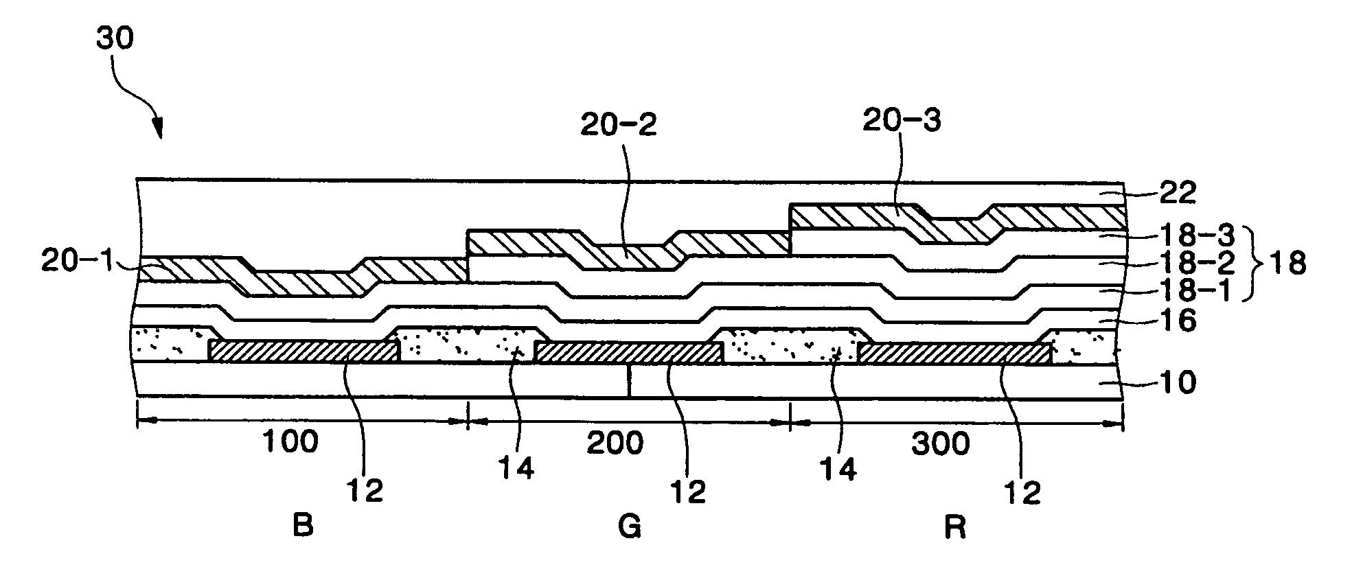
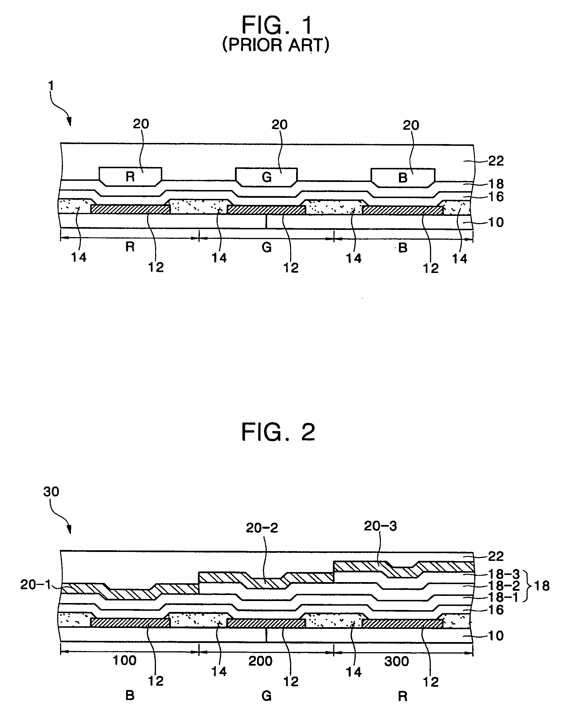
[0023] The embodiments of the invention and the various features and advantageous details thereof are explained more fully with reference to the non-limiting embodiments and examples that are described and-or illustrated in the accompanying drawings and detailed in the following description. It should be noted that the features illustrated in the drawings are not necessarily drawn to scale, and features of one embodiment may be employed with other embodiments as the skilled artisan would recognize, even if not explicitly stated herein.

[0024] Descriptions of well-known components and manufacturing techniques may be omitted so as to not unnecessarily obscure the embodiments of the invention. The examples used herein are intended merely to facilitate an understanding of ways in which the invention may be practiced and to further enable those of skill in the art to practice the embodiments of the invention. Accordingly, the examples and embodiments herein should not be construed as lim...


PUM


Abstract

An organic light emitting display device may include: a substrate having first, second and third pixel regions. A first electrode layer may be formed in each of the first, second and third pixel regions on the substrate. A hole injection layer may be formed over an entire surface of the substrate on the first electrode layers. A first hole transport layer may be formed on the first electrode layers in the first, second and third pixel region. A second hole transport layer may be formed on the first hole transport layer in any two adjacent pixel regions among the first, second and third pixel regions. A third hole transport layer may be formed on the second hole transport layer in any one of the two adjacent pixel region. A first, second and third organic emission layers may be formed on the first, second and third hole transport layer. A second electrode layer may be formed on the first, second and third organic emission layers. An OLED configured in this or a similar manner benefits from uniform operating characteristics and reducing tac time.

Description

CROSS-REFERENCE TO RELATED APPLICATIONS [0001] This application claims priority to Korean Patent Application No. 2004-45724, filed Jun. 18, 2004, the disclosure of which is incorporated herein by reference in its entirety. BACKGROUND OF THE INVENTION [0002] 1. Field of the Invention [0003] The present invention relates to an organic light emitting display device (OLED) and method of fabricating the same and, more particularly, to an easily fabricated organic light emitting display device having uniform display characteristics and method of fabricating the same. [0004] 2. Description of the Related Art [0005] Active and passive matrix OLEDs incorporate thin film transistors and have attracted attention in recent years as providing an alternative to cathode ray tube (CRT) devices because OLEDs offer wider viewing angle, better contrast, and faster response speed. [0006] OLEDs may be classified as organic or inorganic depending on the type of electroluminescent (EL) material used to fo...

Claims


Application Information

Patent Timeline
IPC IPC(8): G09F9/30H01L27/32H05B33/26H01L51/50H01L51/52H05B33/10H05B33/12H05B33/14
CPCH01L27/3211H01L2251/558H01L51/5265H01L51/5048H10K59/35H10K50/14H10K2102/351H05B33/26H10K50/852
Inventor LEE, KWAN-HEEKWON, JANG-HYUKRYU, SEOUNG-YOON
Owner SAMSUNG DISPLAY CO LTD
Why Eureka
Try Eureka