

Electron emission device and method for manufacturing the same
- Summary
- Abstract
- Description
- Claims
- Application Information
AI Technical Summary
Benefits of technology
Problems solved by technology
Method used
Image

Examples
Embodiment Construction
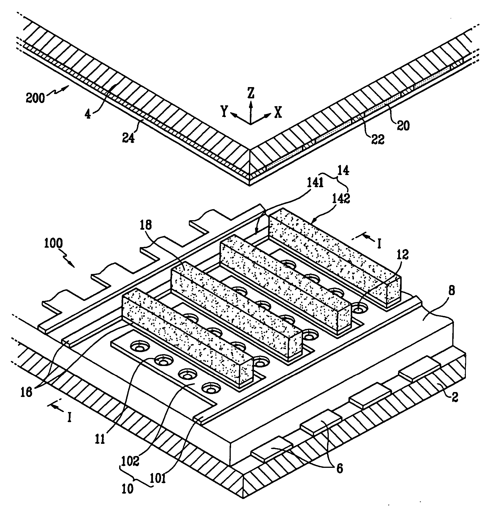
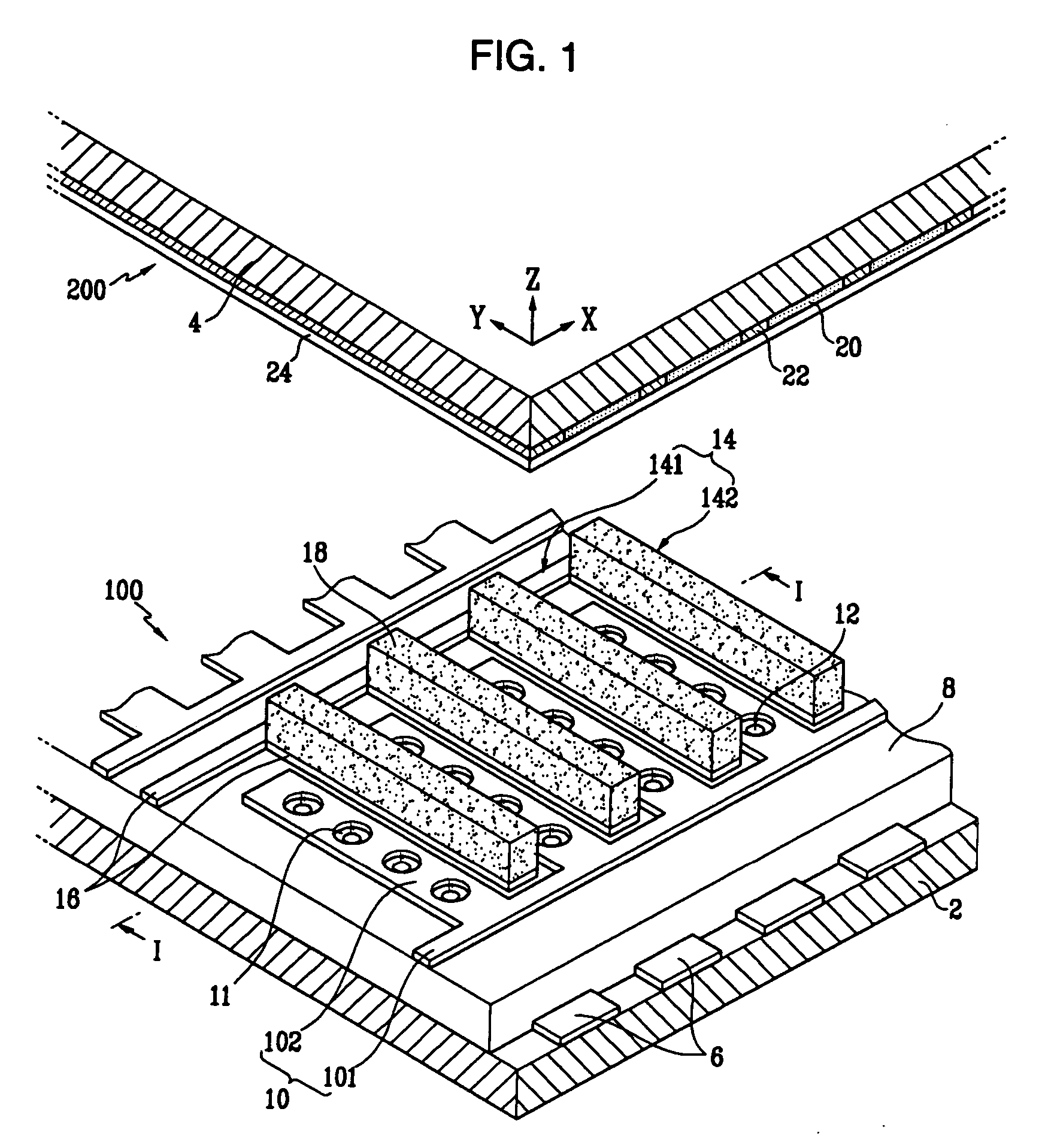
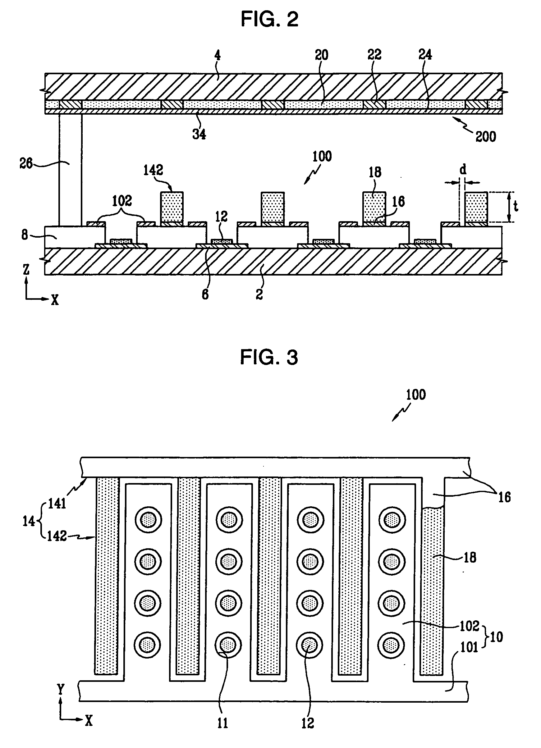
[0026] FIGS. 1 to 3 show different views of an electron emission device, avvording to one embodiment of the present invention. As shown in FIGS. 1 to 3, the electron emission device includes first and second substrates 2 and 4 arranged parallel to each other with a predetermined distance. A sealing member (not shown) is provided at the peripheries of the first and the second substrates 2 and 4, thereby forming a vacuum inner space in association with the first and the second substrates 2 and 4.
[0027] An electron emission unit 100 is provided on a surface of the first substrate 2 facing the second substrate 4 to emit electrons toward the second substrate 4. A light emission unit 200 is provided on a surface of the second substrate 4 facing the first substrate 2 to emit visible rays due to the electrons.
[0028] Cathode electrodes 6 are stripe-patterned on the first substrate 2 in a direction of the first substrate 2, and an insulating layer 8 is formed on the entire surface of the fi...
PUM
 Abstract
Description
Claims
Application Information