
Application-specific integrated circuit equivalents of programmable logic and associated methods

a technology of integrated circuits and programmable logic, applied in the direction of computation using denominational number representation, pulse technique, instruments, etc., can solve the problems of ineffective waste of substantial amounts of circuitry in less-than-fully-used les, complex and/or extensive logic or logic-type operations, etc., to facilitate the conversion of an fpga design and save time and cost.

Inactive Publication Date: 2006-01-05
ALTERA CORP
View PDF15 Cites 37 Cited by
  • Summary
  • Abstract
  • Description
  • Claims
  • Application Information

AI Technical Summary

Benefits of technology

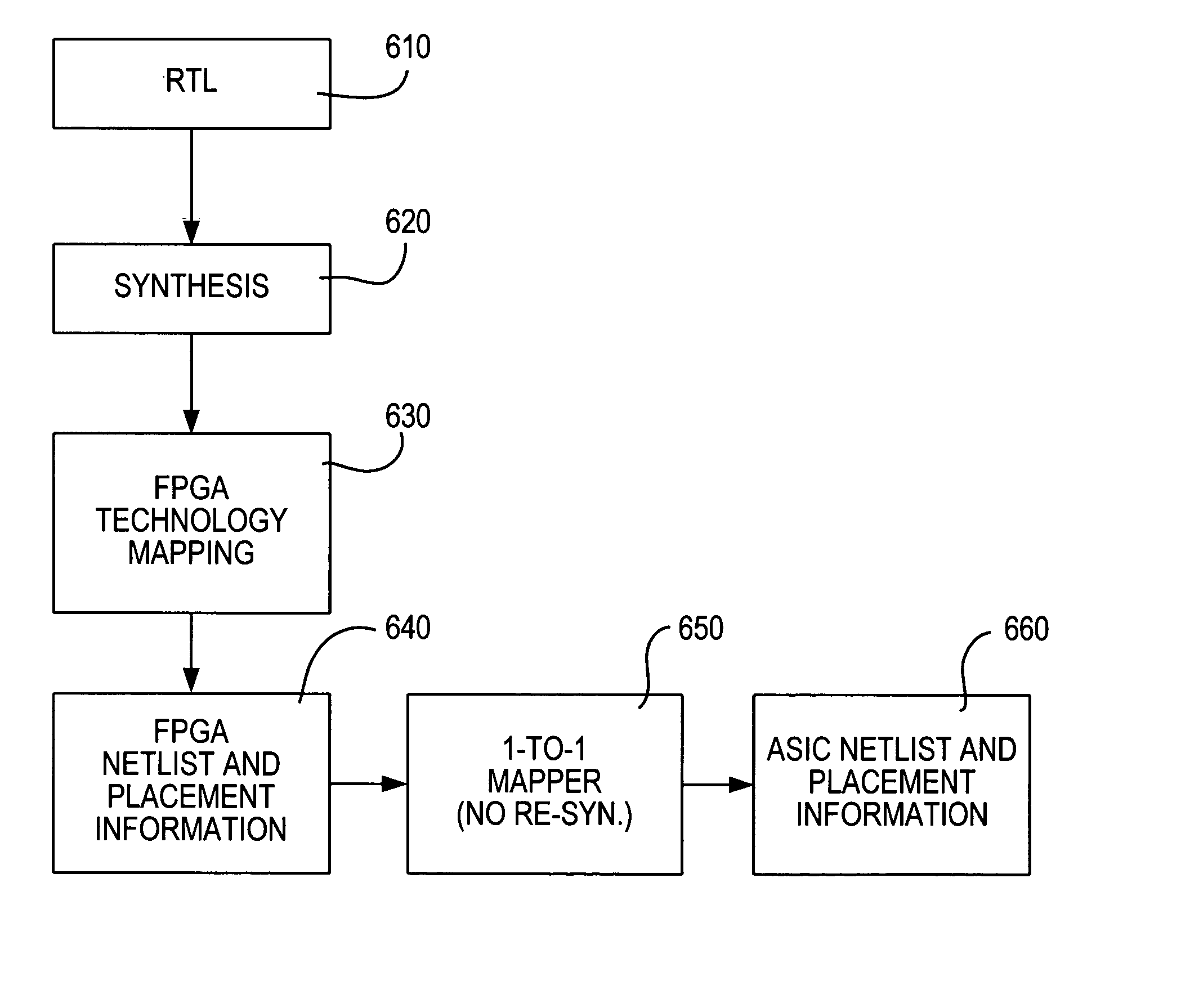
[0007] At least to a large extent, there is preferably a one-for-one correspondence between each LE and the equivalent HLE or group of HLEs. This facilitates converting an FPGA design to the equivalent ASIC, and also vice versa, without re-synthesis of the user's logic. Avoiding such re-synthesis can save time and cost, and it also gives greater assurance that the ASIC and FPGA equivalents will function substantially identically and without fault (assuming that either the FPGA or the ASIC has been proven to function properly).

Problems solved by technology

In addition to many LEs, an FPGA also typically has programmable routing circuitry for conveying signals to, from, and / or between the LEs in any of many different ways so that very complex and / or extensive logic or logic-type operations can be performed by combining or otherwise using multiple LEs.
For example, most user designs do not make use of all the circuitry on an FPGA.
In any of these cases, substantial amounts of the circuitry in the less-than-fully-utilized LEs is effectively wasted.

Method used


Image

  • Application-specific integrated circuit equivalents of programmable logic and associated methods
  • Application-specific integrated circuit equivalents of programmable logic and associated methods
  • Application-specific integrated circuit equivalents of programmable logic and associated methods

Examples


Embodiment Construction

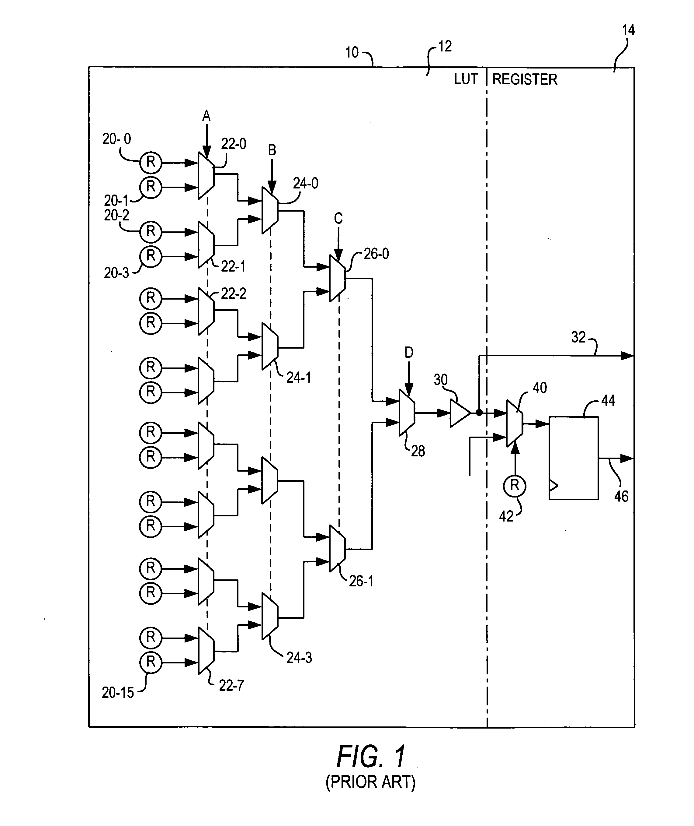
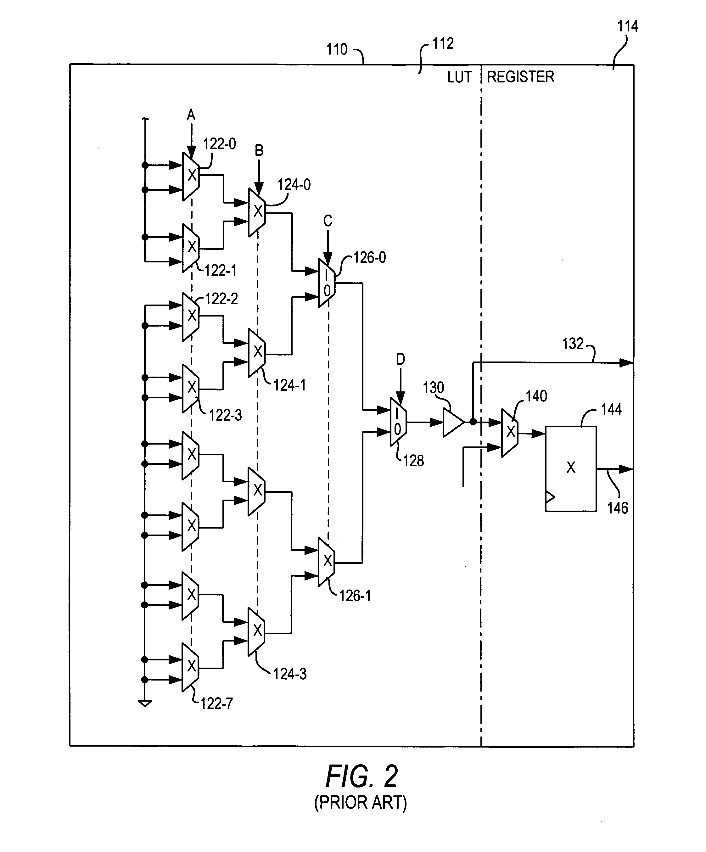
[0025] An illustrative, known, FPGA LE 10 is shown in FIG. 1. LE 10 includes a 4-LUT portion 12 and a register portion 14. 4-LUT portion 12 includes 16 programmable memory (e.g., RAM) cells 20-0 through 20-15. The outputs of RAM cells 20 are applied, in respective pairs, to the inputs of eight two-input multiplexers (“muxes”) 22-0 through 22-7. 4-LUT input A controls which of its inputs (from RAM cells 20) each of muxes 22 selects to be its output. For example, if input A is logic 1, each of muxes 22 selects its upper input to be its output. If input A is logic 0, each of muxes 22 selects its lower input to be its output. The outputs of muxes 22 are applied, in respective pairs, to the inputs of four two-input muxes 24. 4-LUT input B controls which of its inputs each of muxes 24 selects as its output. Again, if B is logic 1, muxes 24 select their upper inputs to output. If B is logic 0, muxes 24 select their lower inputs to output. The outputs of muxes 24 are applied, in respective ...


PUM


Abstract

Providing ASIC equivalents of FPGAs is facilitated and made more efficient and economical by using an ASIC architecture including a plurality of so-called hybrid logic elements (“HLEs”), each of which can provide a portion of the full functionality of an FPGA logic element (“LE”). The functionality of each FPGA LE implementing a user's logic design can be mapped to one or more HLEs without re-synthesis of the user's logic. Only as many HLEs as are necessary are used to perform the functions of each LE. The one-for-one equivalence between each LE and either (1) one HLE or (2) a group of HLEs facilitates mapping (without re-synthesis) in either direction between FPGA and ASIC designs.

Description

BACKGROUND OF THE INVENTION [0001] This invention relates to circuitry for application-specific integrated circuits (“ASICs”) that can be used as equivalents of or substitutes for programmable logic circuitry (PLDs or FPGAs). The invention also relates to transferring designs for particular uses of an ASIC or a PLD (or FPGA) between those two types of devices so that device interchangeability is achieved. [0002] A typical programmable logic device (“PLD”) or field-programmable gate array (“FPGA”) includes many logic elements (“LEs”) of a fixed size. (For convenience herein, the term FPGA is used as a generic term for PLDs and FPGAs.) For example, an FPGA LE may include a four-input look-up table (“LUT”), a register, and some routing circuitry that allows the register to be either used (e.g., to register the output of the LUT) if sequential logic or operation is desired, or to be bypassed by the LUT output if only combinational or combinatorial logic or operation is desired. An FPGA ...

Claims


Application Information

Patent Timeline
Patent Type & Authority Applications(United States)
IPC IPC(8): G06F7/38H03K19/173G06F17/50
CPCH03K19/177H03K19/1737
Inventor CHUA, KAR KENGCHEUNG, SAMMYPHOON, HEE KONGTAN, KIM PINGOAY, WEI LIAN
Owner ALTERA CORP
Learn More