Multi-chip image sensor package module

a multi-chip, image sensor technology, applied in the direction of instruments, photoelectric discharge tubes, electric discharge lamps, etc., can solve the problems of thicker package modules and higher packaging costs, and achieve the effects of thin modules, reduced packaging costs, and thin packages

Inactive Publication Date: 2006-01-26
ADVANCED SEMICON ENG INC
View PDF9 Cites 50 Cited by
  • Summary
  • Abstract
  • Description
  • Claims
  • Application Information

AI Technical Summary

Benefits of technology

[0013] In the multi-chip image sensor package module 100 mentioned above, the image sensor chip 130 is located between the substrate 110 and the IC chip 120 inside a composite chip cavity to achieve a thin module. Preferably, the package module 100 includes a filling material 170, such as a non-flow underfilling material, a non-conductive paste (NCP), or an anisotropic conductive paste (ACP). The filling material 170 is formed between the mounting surface 121 of the IC chip 120 and the lower surface 112 of the substrate 110 without contaminating the sensing region 133 of the image sensor chip 130 to encapsulate the bumps 122 and seal the image sensor chip 130. Therefore, the image sensor chip 130 is surrounded by an airtight space formed by the IC chip 120, the filling material 170, the opening 113 of the substrate 110 and the lens module 140 so that a thinner package module with lower package cost and excellent yield can be achieved.
[0014] According to the second embodiment of the present invention, as shown in FIG. 2. A multi-chip image sensor package module 200 mainly includes a substrate 210 having a opening 213, an IC chip 220, an image sensor chip 230 and a glass cover 241. The opening 213 passes through the upper surface 211 and the lower surface 212 of the substrate 210, and is larger than the image sensor chip 230 in size. A mounting base 242 connecting the glass cover 241 is mounted on the upper surface 211. The substrate 210 has a protruding layer 214 which is formed on periphery of the lower surface 212 for accommodating the IC chip 220. Moreover, the opening 213 of the substrate 210 has a stepping portion 215 toward the lower surface 212. The image sensor chip 230 is flip-chip mounted on the stepping portion 215 via a plurality of flip-chip bumps 234. The IC chip 220 is also mounted on the lower surface 212 inside the protruding layer 214. The IC chip 220 has a mounting surface 221 which includes a central region 223 and a peripheral region 224. A plurality of bumps 222 are formed at the peripheral region 224 of the mounting surface 221 without blocking the central region 223. The bumps 222 are connected on the lower surface 212 of the substrate 210. A chip cavity consists of the central region 223 of the IC chip 220, the bumps 222 and the opening 213 of the substrate 210 for accommodating the image sensor chip 230. The image sensor chip 230 has an active surface 231 and a backside surface 232. The active surface 231 includes a sensing region 233 smaller than the opening 213 of the substrate 210. The image sensor chip 230 includes a plurality of bumps 234, so that the image sensor chip 230 can be flip-chip mounted on the stepping portion 215 of the substrate 210. The image sensor...

Problems solved by technology

The package module is thicke...

Method used


Image

  • Multi-chip image sensor package module
  • Multi-chip image sensor package module
  • Multi-chip image sensor package module

Examples


first embodiment

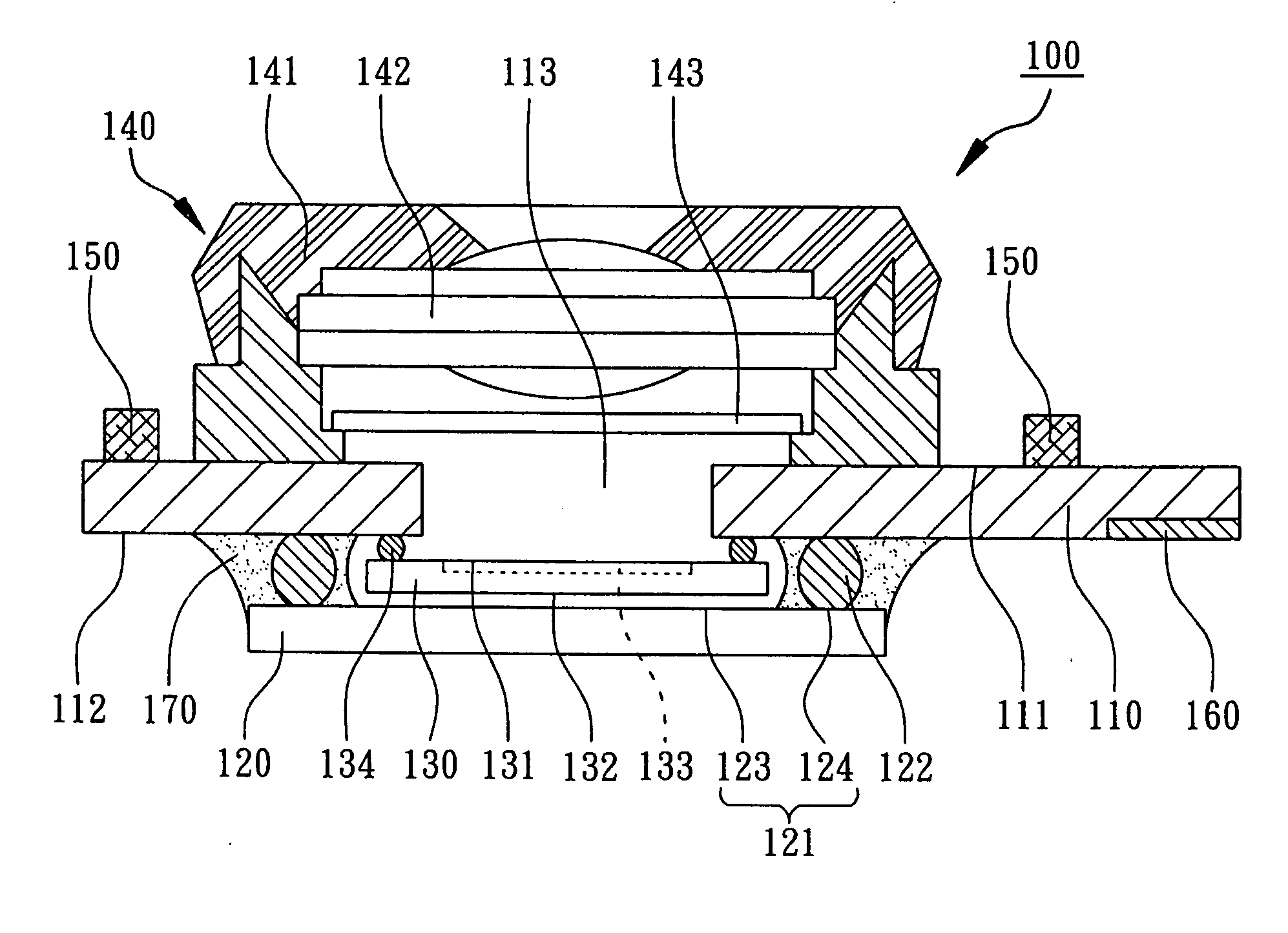
[0009] According to the present invention, a multi-chip image sensor package module 100 is illuminated as shown in FIG. 1, which mainly includes a substrate 110, an IC chip 120 and an image sensor chip 130 and a lens 142. The substrate 110 may have a multi-layer circuits structure, such as a multi-layer co-fired ceramic, a MLCC, a printed circuited board (PCB), or a leadframe-based circuit board, for electrical connection of the IC chip 120 and the image sensor chip 130. The substrate 110 has an upper surface 111, a lower surface 112, and an opening 113 through the upper surface 111 and the lower surface 112.

[0010] According to the present embodiment, the IC chip 120 may be a flip chip or a chip scale package (CSP). The IC chip 120 has a mounting surface 121 and includes a plurality of bumps 122 formed on the mounting surface 121 of the IC chip 120. In this embodiment, the IC chip 120 is a DSP (Digital Signal Processor). The IC chip 120 is flip-chip mounted on the lower surface 112 ...

second embodiment

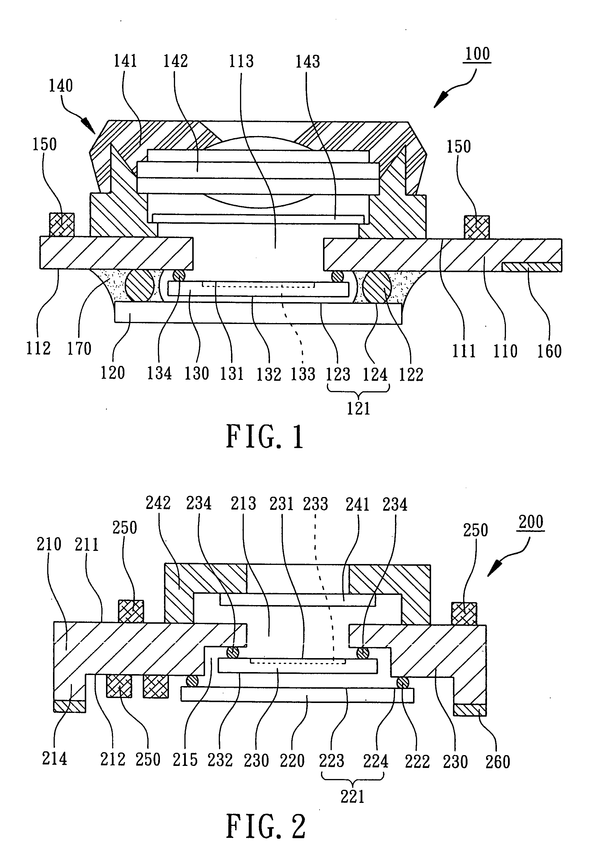
[0014] According to the present invention, as shown in FIG. 2. A multi-chip image sensor package module 200 mainly includes a substrate 210 having a opening 213, an IC chip 220, an image sensor chip 230 and a glass cover 241. The opening 213 passes through the upper surface 211 and the lower surface 212 of the substrate 210, and is larger than the image sensor chip 230 in size. A mounting base 242 connecting the glass cover 241 is mounted on the upper surface 211. The substrate 210 has a protruding layer 214 which is formed on periphery of the lower surface 212 for accommodating the IC chip 220. Moreover, the opening 213 of the substrate 210 has a stepping portion 215 toward the lower surface 212. The image sensor chip 230 is flip-chip mounted on the stepping portion 215 via a plurality of flip-chip bumps 234. The IC chip 220 is also mounted on the lower surface 212 inside the protruding layer 214. The IC chip 220 has a mounting surface 221 which includes a central region 223 and a ...

third embodiment

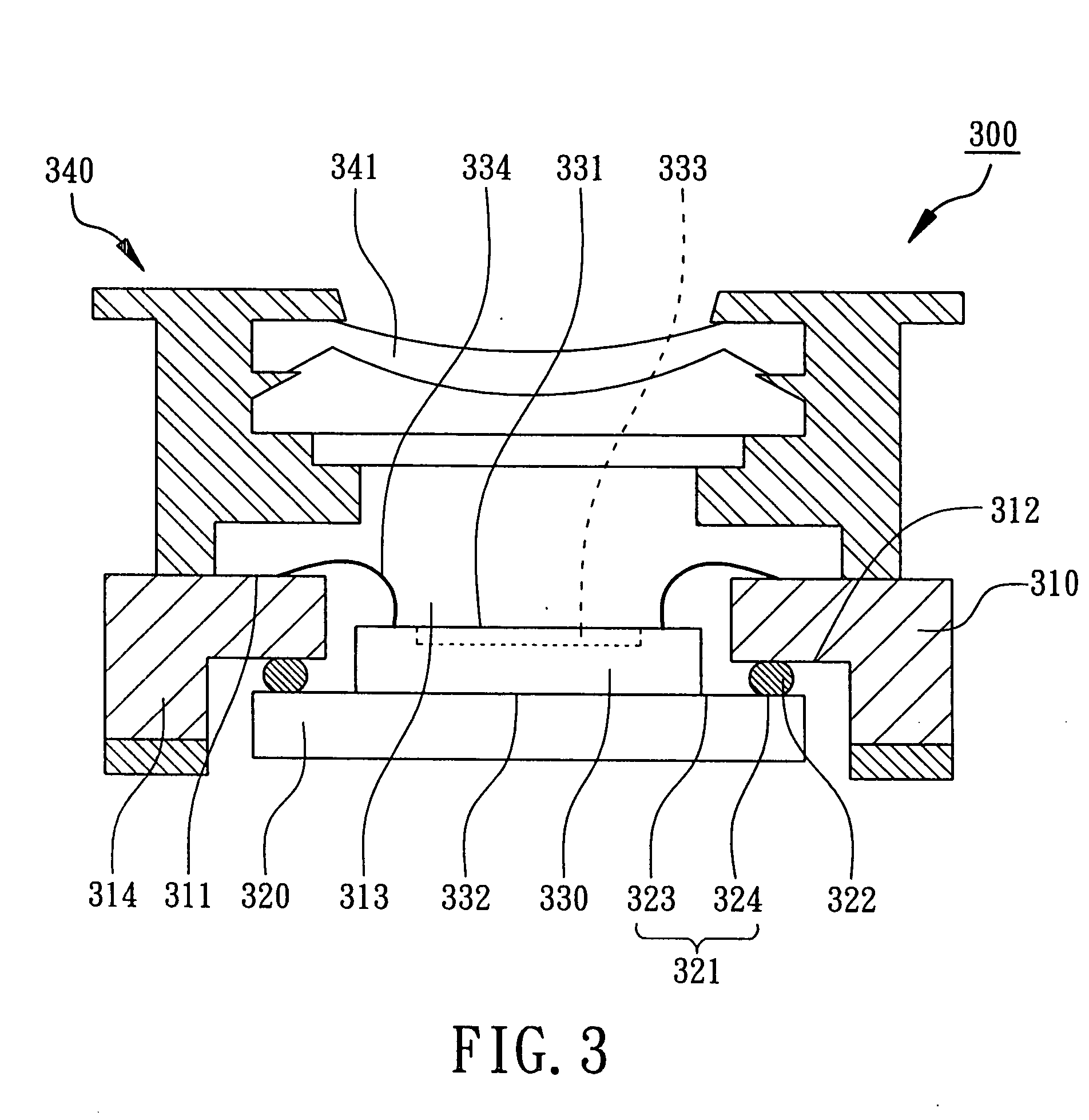
[0015] According to the present invention, as shown in FIG. 3. A multi-chip image sensor package 300 mainly includes a substrate 310 having an opening 313, an IC chip 320, and an image sensor chip 330. The opening 313 of the substrate 310 passes through the upper surface 311 and the lower surface 312. The opening 313 is smaller than the sensing region 333 of the image sensor chip 330. In this embodiment, the opening 313 is larger than the active surface 331 of the image sensor chip 330. A lens module 340 having a lens 341 can be mounted on the upper surface 331 of the substrate 310. Preferably, the substrate 310 comprises a protruding layer 314 which is formed on the lower surface 312 for accommodating the IC chip 320. The IC chip 320 has a mounting surface 321 which includes a central region 323. A plurality of bumps 322 are formed at the peripheral region 324 of the mounting surface 321 without blocking the central region 323. The bumps 322 connect the lower surface 312 of the sub...


PUM


Abstract

A multi-chip image sensor package module includes a substrate having an opening, an IC chip, an image sensor chip and a glass cover. The IC chip includes a plurality of bumps on its mounting surface to mount on the lower surface of the substrate. The glass cover is disposed above the upper surface of the substrate. The image sensor chip is disposed between the mounting surface of the IC chip and the upper surface of the substrate by chip-to-chip attachment or flip-chip connection in a manner that the sensing region of the image sensor chip is aligned with the glass cover or a lens through the opening. Thus the multi-chip image sensor package module can have a thinner profile with lower assemble cost.

Description

FIELD OF THE INVENTION [0001] The present invention relates to an image sensor package module, and more particularly to a multi-chip image sensor package module for accommodating an image sensor chip at low cost. BACKGROUND OF THE INVENTION [0002] Conventionally, an image sensor chip is integrated in a package module with other IC chips such as digital signal processor, IC, for electrical integrity. However, the dimension and thickness of the package module will increase. As disclosed in U.S. Pat. No. 6,686,588, a conventional image sensor package module includes an image sensor chip and electronic components connected to a substrate. The image sensor chip is attached to the upper surface of the substrate by adhesive. A sidewall with locking features is mounted on the upper surface to form a chip cavity for accommodating the image sensor chip and to assemble with a lens housing. The electronic components and solder balls are disposed on the lower surface of the substrate to form a p...

Claims


Application Information

Patent Timeline
IPC IPC(8): H01J40/14
CPCH01L31/0203H01L31/0232H01L2224/48091H01L2924/00014H01L31/02325
Inventor YANG, JUN-YOUNGHAN, JONG-HOLEE, JUN-HONG
Owner ADVANCED SEMICON ENG INC
Why Eureka
Try Eureka