Encapsulation of conductive lines of semiconductor devices

a technology of conductive lines and semiconductor devices, applied in the manufacture/treatment of galvano-magnetic devices, semiconductor devices, electrical apparatus, etc., can solve the problems of difficult direct patterning or etching of copper, difficult to use exposed copper lines and vias, and many of the more effective processing steps are simply too harsh to be used with such exposed copper lines. , to achieve the effect of reducing the effective dielectric constant and capacitance of the structure, reducing the surface temperature and reducing the s

Inactive Publication Date: 2006-01-26
INFINEON TECH AG +1
View PDF5 Cites 12 Cited by
  • Summary
  • Abstract
  • Description
  • Claims
  • Application Information

AI Technical Summary

Benefits of technology

[0011] The methods and semiconductor devices described herein comprise a substrate with a dielectric having a top surface that defines at least one area of metallization having an exposed top surface such as is provided by a typical copper damascene process. For many applications, the area of metallization formed by the damascene process will also include a barrier liner covering the sides and bottom of the cavity, trench, or via before the copper or other metal is deposited. Suitable materials for the barrier liner include, but are not necessarily limited to, Tantalum (Ta), Tantalum Nitride (TaN), Titanium (Ti), Titanium Nitride (TiN), Silicon Nitride (SiN), and Silicon Carbide (SiC), as examples. A planar layer of encapsulating protective material, such as TaN, Ta, Ti, TiN, or combinations thereof, as examples, is then deposited over at least the top surface of the area of metallization to encase or encapsulate the area of metallization. The layer of encapsulating protective material may be planarized by a CMP (Chemical Mechanical Polish) to provide a very smooth top surface for the formation of subsequently deposited materials and devices, for example. The planarized encapsulated or protected areas of metallization provide a s

Problems solved by technology

Because MRAM devices operate differently than traditional memory devices and because they are relatively new, they introduce design and manufacturing challenges.
Copper is difficult to directly pattern or etch, and thus, damascene processes are typically used to form copper interconnects.
Exposed copper lines and vias are particularly susceptible to corrosion resulting from subsequent processing steps.
Consequently, many of the more effective proces

Method used


Image

  • Encapsulation of conductive lines of semiconductor devices
  • Encapsulation of conductive lines of semiconductor devices
  • Encapsulation of conductive lines of semiconductor devices

Examples


Embodiment Construction

[0017] The making and using of the presently preferred embodiments are discussed in detail below. It should be appreciated, however, that the present invention provides many applicable inventive concepts that can be embodied in a wide variety of specific contexts. The specific embodiments discussed are merely illustrative of specific ways to make and use the invention, and do not limit the scope of the invention.

[0018] The present invention will be described with respect to preferred embodiments in a specific context, namely an MRAM device. The invention may also be applied, however, to other semiconductor devices, and has particular useful application when magnetic materials are used as material layers, for example.

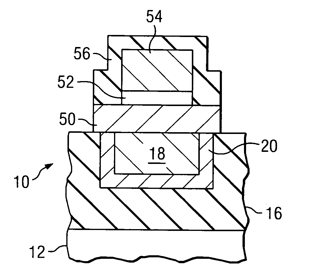
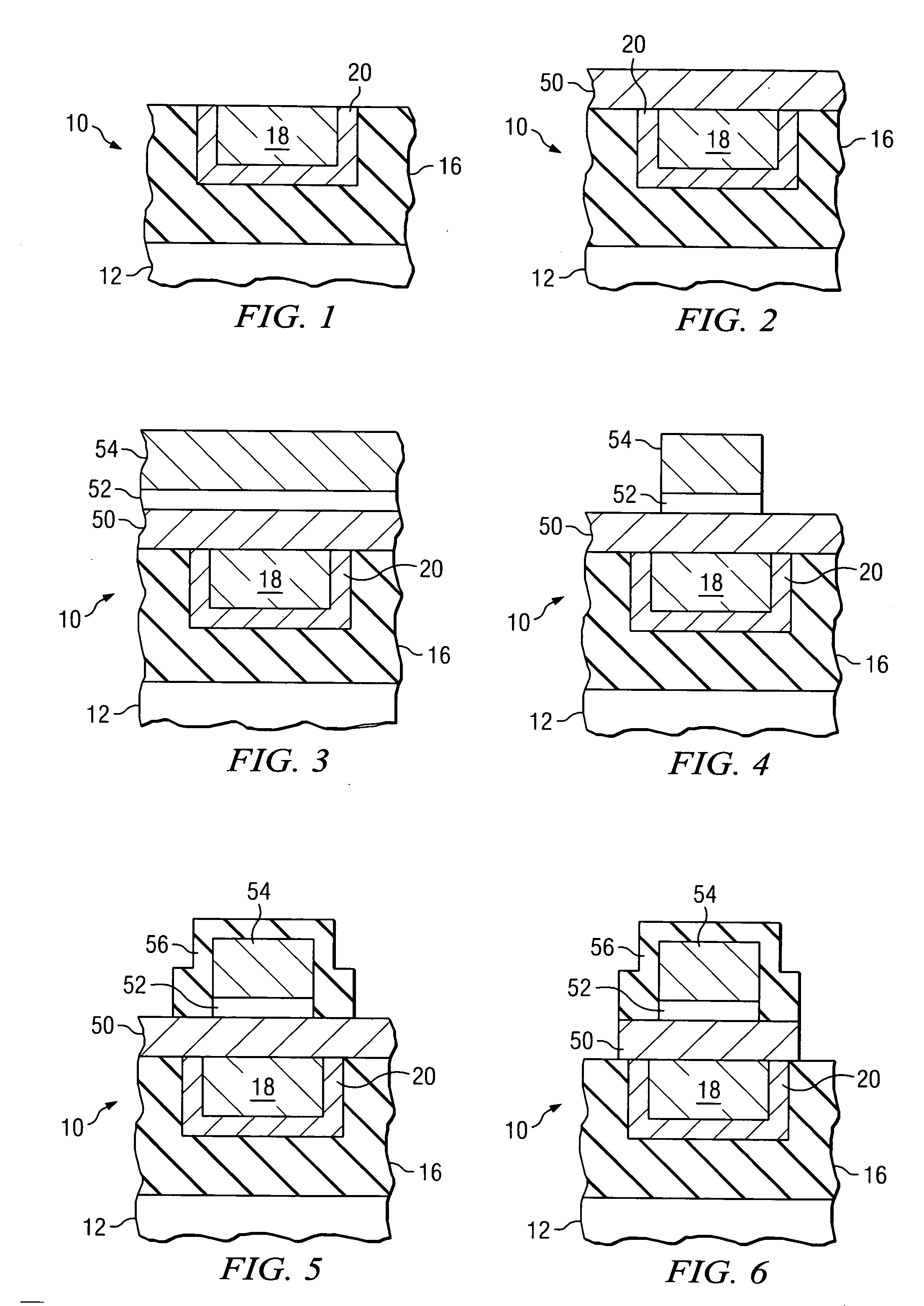
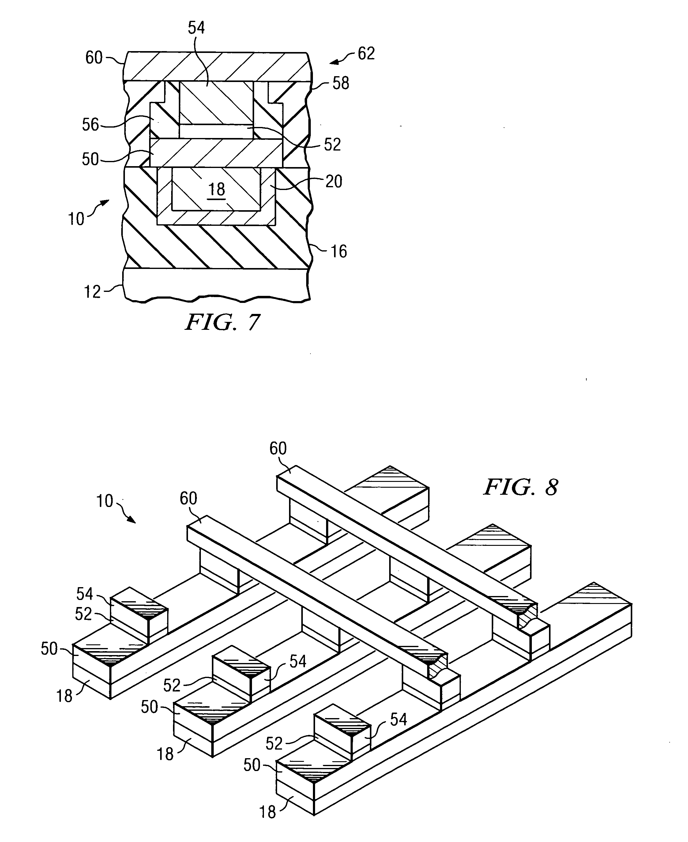
[0019] In U.S. patent application Ser. No. 10 / 610,609, filed on Jul. 1, 2003, entitled, “Recessed Metal Lines for Protective Enclosure in Integrated Circuits,” which is incorporated herein by reference, methods of recessing damascene conductive lines and filling the re...


PUM


Abstract

A method of encapsulating conductive lines of semiconductor devices and a structure thereof. An encapsulating protective material comprising TaN, Ta, Ti, TiN, or combinations thereof is disposed over conductive lines of a semiconductor device. The encapsulating protective material protects the conductive lines from harsh etch chemistries when a subsequently deposited material layer is patterned and etched. The encapsulating protective material is conductive and may be left remaining in the completed semiconductor device. The encapsulating material is patterned using a masking material, and processing of the semiconductor device is then continued. The masking material may be left remaining in the structure as part of a subsequently deposited insulating material layer.

Description

CROSS-REFERENCE TO RELATED APPLICATIONS [0001] This application relates to the following co-pending and commonly assigned patent application Ser. No. 10 / 610,609, filed on Jul. 1, 2003, entitled, “Recessed Metal Lines for Protective Enclosure in Integrated Circuits,” which application is hereby incorporated herein by reference.TECHNICAL FIELD [0002] The present invention relates generally to semiconductor devices, and more particularly to protecting conductive lines while patterning subsequently deposited material layers. BACKGROUND [0003] A recent development in semiconductor memory devices involves spin electronics, which combines semiconductor technology and magnetics. The spin of electrons, rather than the charge, is used to indicate the presence of binary states “1” and “0.” One such spin electronic device is a magnetic random access memory (MRAM) device, which includes conductive lines (wordlines and bitlines) positioned in a different direction, e.g., perpendicular to one anot...

Claims


Application Information

Patent Timeline
IPC IPC(8): H01L21/48
CPCH01L43/12H01L27/222H10B61/00H10N50/01
Inventor KASKO, IHARLOW, KIA-SENGHUMMEL, JOHN P.
Owner INFINEON TECH AG
Why Eureka
Try Eureka