Reduction of field edge thinning in peripheral devices

Inactive Publication Date: 2006-01-26
MICRON TECH INC
View PDF12 Cites 5 Cited by
  • Summary
  • Abstract
  • Description
  • Claims
  • Application Information

AI Technical Summary

Benefits of technology

[0021]FIG. 22 is a flow chart of another embodiment of a fabrication process th

Problems solved by technology

More uniform gate oxides leads to les

Method used


Image

  • Reduction of field edge thinning in peripheral devices
  • Reduction of field edge thinning in peripheral devices
  • Reduction of field edge thinning in peripheral devices

Examples


Embodiment Construction

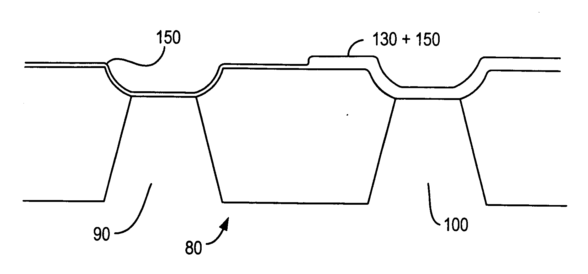
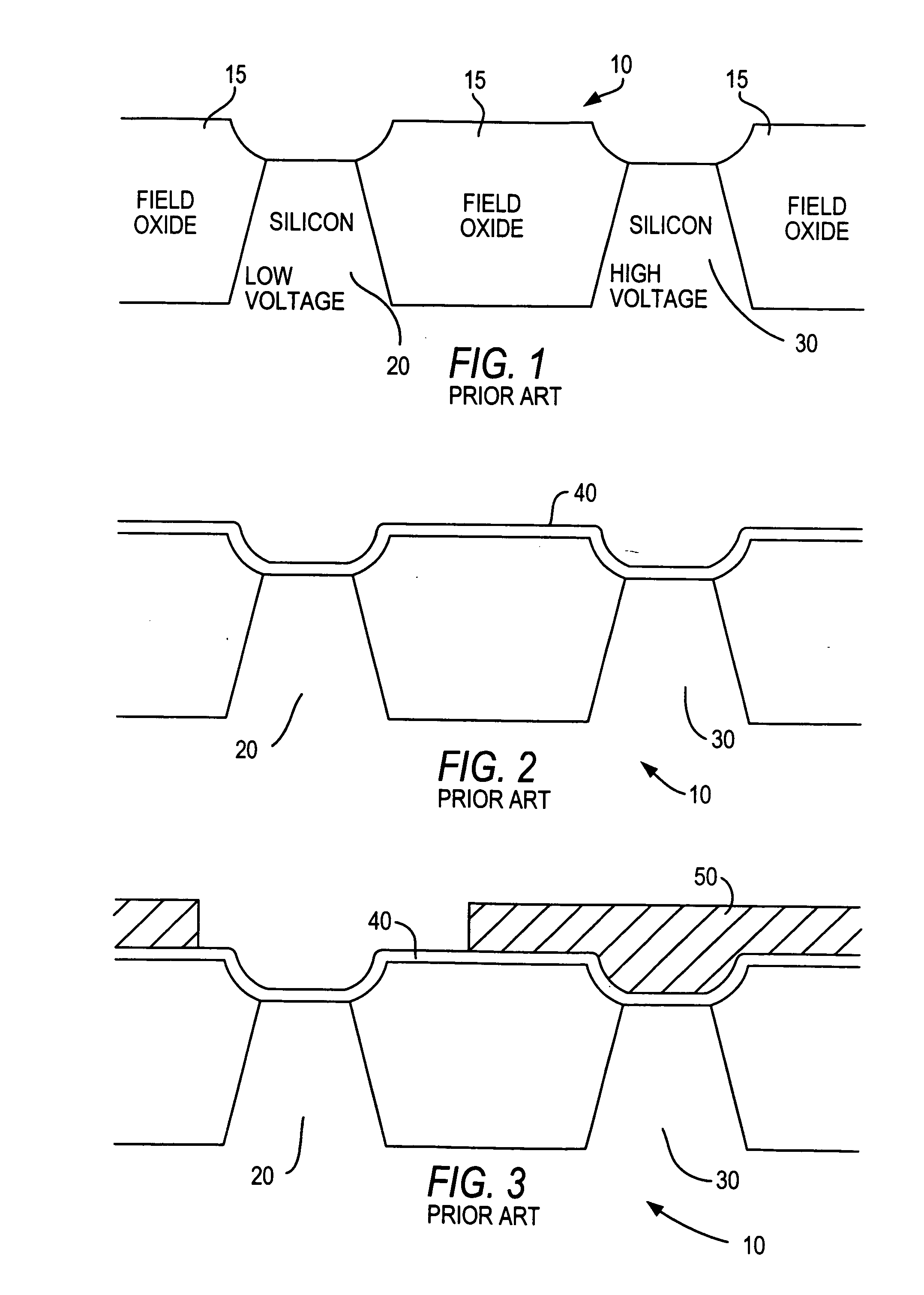
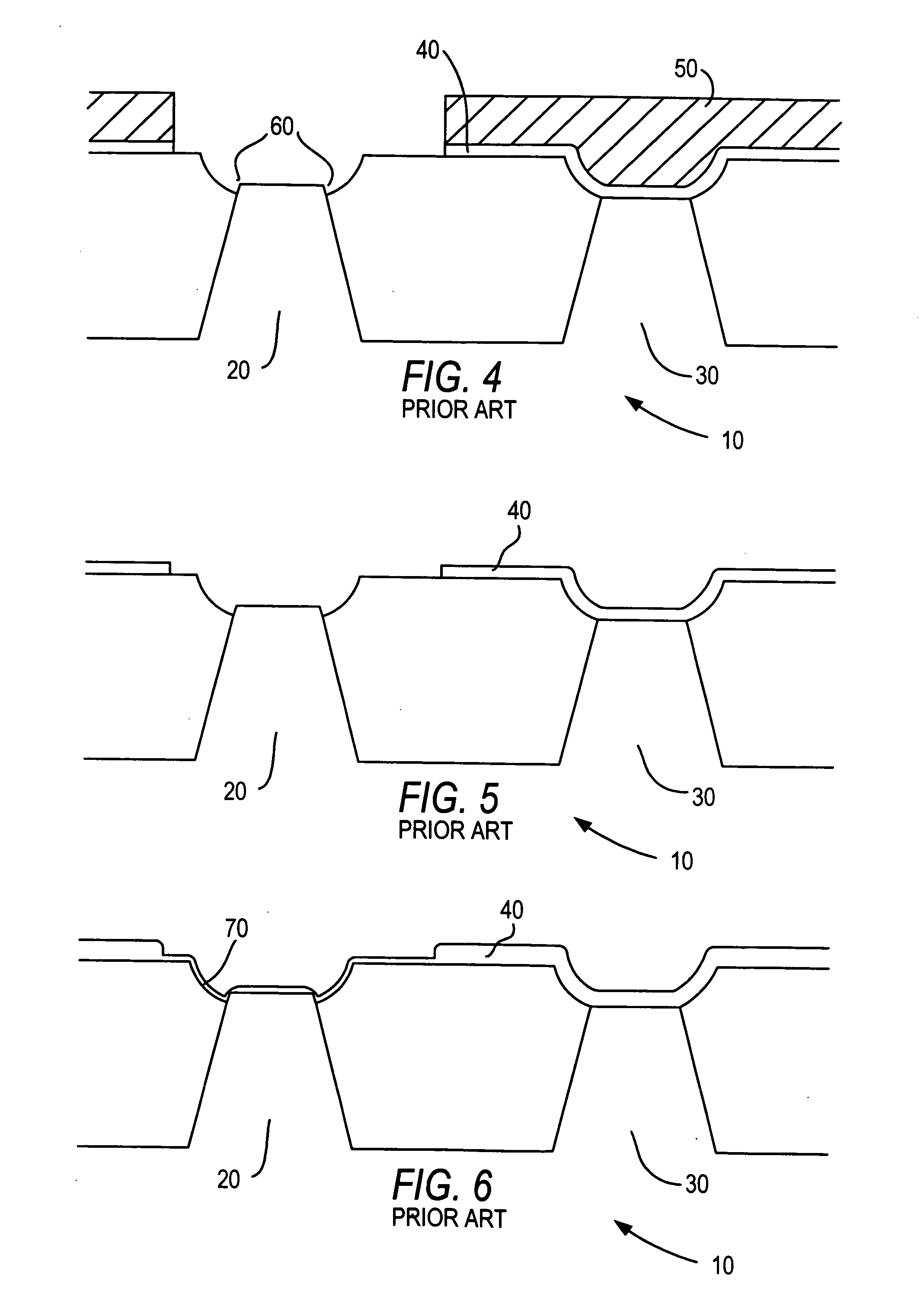
[0022] The invention is directed to the fabrication of peripheral devices. Peripheral devices may be used to implement storage cells in memory devices such as, for example, SRAMs, DRAMs, and memory devices used in flash applications.

[0023] In the fabrication of some peripheral memory devices, a dielectric layer is deposited over the peripheral devices and the memory devices to which the peripheral devices are coupled. The dielectric layer may be an interpoly dielectric layer. Such an interpoly dielectric layer may be, for example, oxide-nitride-oxide or aluminum-oxide. The dielectric is used as an oxidation and wet-oxide etch barrier. In some peripheral device fabrication, the dielectric layer is removed from the entire peripheral device but not the memory device. The dielectric layer is removed from the peripheral device to allow thin and thick gate oxides to be grown over the peripheral device. That is, the low and high voltage devices are exposed before the growth of the thin an...


PUM

PropertyMeasurementUnit
Thicknessaaaaaaaaaa
Dielectric polarization enthalpyaaaaaaaaaa
Electric potential / voltageaaaaaaaaaa

Abstract

A dielectric layer (e.g., an interpoly dielectric layer) is deposited over low and high voltage devices of a peripheral memory device. The dielectric behaves as an oxidation and wet oxide etch barrier. The dielectric prevents the devices from being stripped by a wet oxide etch that can result in the exposure of the silicon corners. The exposure of a silicon corner may increase thinning of a gate oxide at the field edge. This causes variability and unreliability in the device. The dielectric is not removed from a device until the device is ready for processing. That is, the dielectric remains on a device until the growing of a gate oxide on that device has begun. This reduces the exposure of the silicon corner. Hedges that result may be removed by exposing a trench in the field oxide at the hedge.

Description

CROSS-REFERENCE TO RELATED APPLICATION [0001] This application is a division of U.S. patent application Ser. No. 10 / 180,415, filed Jun. 24, 2002, which is hereby incorporated by reference herein in its entirety.BACKGROUND OF THE INVENTION [0002] This invention relates to reducing gate oxide thinning at the field edge of complimentary metal oxide semiconductor (CMOS) devices and, more particularly, to reducing field edge thinning in peripheral devices. [0003] Some CMOS devices are fabricated in such a way that a thin gate oxide and a thick gate oxide are grown on the device. In some processes for fabricating these peripheral CMOS devices, the thin gate oxide devices are sometimes stripped with a wet oxide etch prior to gate oxidation. In other processes, the thick gate oxide devices are sometimes stripped with a wet oxide etch prior to gate oxidation. When a device is stripped with a wet oxide etch, the silicon corners at the field edges may be exposed. This results in increased gate...

Claims


Application Information

Patent Timeline
IPC IPC(8): H01L21/8234H01L21/762H01L21/8238H01L21/8242H01L27/105H01L27/108
CPCH01L21/76224H01L21/823462H01L21/823481H01L21/823857H01L21/823878Y10T29/41H01L27/10894H01L27/10897H01L27/1052Y10S438/981Y10T29/5313H01L27/105H10B99/00H10B12/50H10B12/09
Inventor WOLSTENHOLME, GRAHAM R.HELM, MARK A.
Owner MICRON TECH INC
Why Eureka
Try Eureka