Wired circuit board

a wired circuit board and circuit board technology, applied in the manufacture of final products, electrical apparatus construction details, instruments, etc., can solve problems such as and achieve the effect of preventing inconsistency in characteristic impedances

Inactive Publication Date: 2006-02-02
NITTO DENKO CORP
View PDF11 Cites 14 Cited by
  • Summary
  • Abstract
  • Description
  • Claims
  • Application Information

AI Technical Summary

Benefits of technology

[0021] According to the wired circuit board of the present invention, the suspension board portion for supporting the magnetic head and the control board portion for controlling the magnetic head are arranged to be continuous and integral with each other, and also the first conductor layer and the second conductor layer are formed from the same material. This arrangement can eliminate the need of providing the connection point for connecting the first conductor layer of the suspension board portion and the second conductor layer of the control board portion at the boundary therebetween. This can provide the result of preventing inconsistency in characteristic impedance at that connection point to allow effective transmission of electrical signals from the magnetic head to the control board portion.

Problems solved by technology

However, electrical resistance changes significantly at connection points between the control circuit board terminal portion 60 and the suspension board terminal portion 62, then causing inconsistency in characteristic impedance thereat.

Method used


Image

  • Wired circuit board
  • Wired circuit board
  • Wired circuit board

Examples


example 1

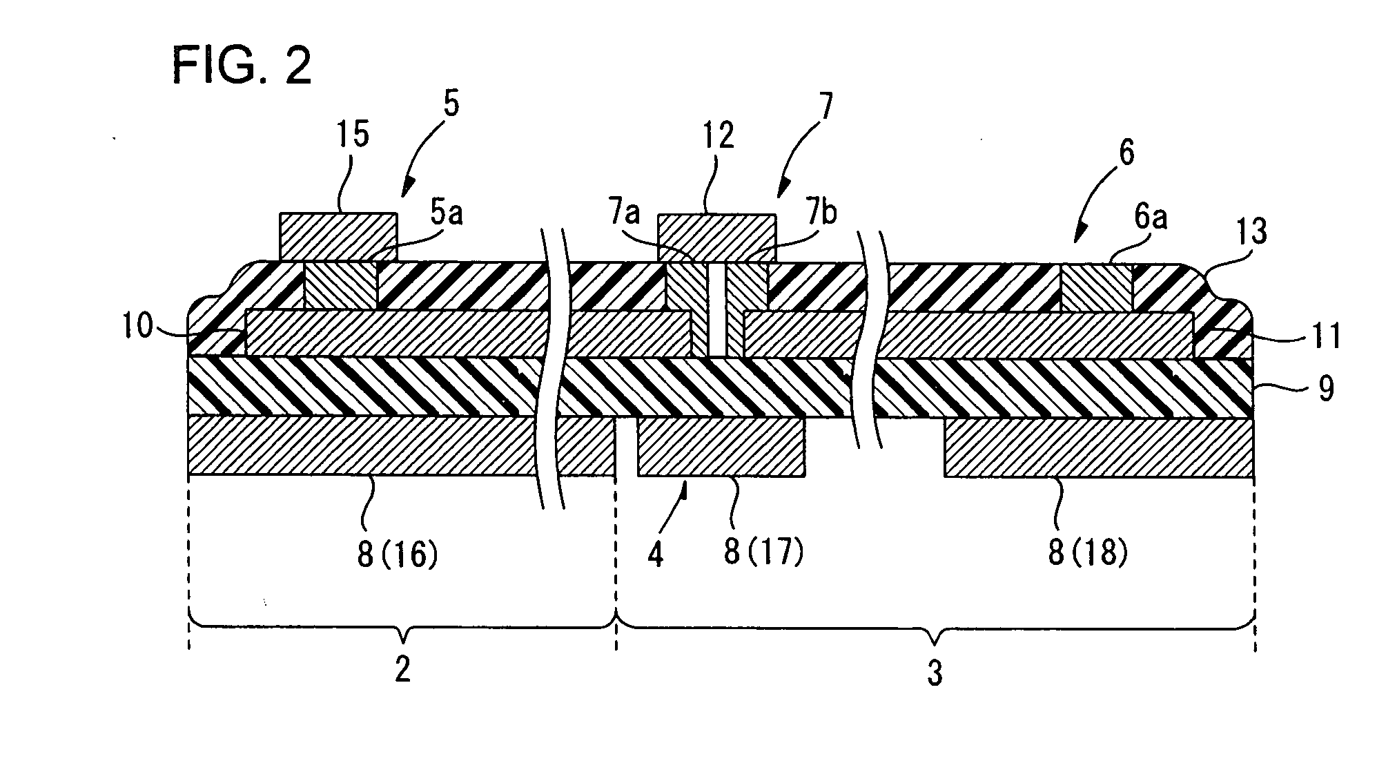
[0068] A metal board of a stainless foil having a thickness of 25 μm (SUS304H-TA) was prepared, first (Cf. FIG. 3(a)). Then, solution of precursor of photosensitive polyimide resin was coated over the metal board so that after dried, it could have thickness of 24 μm. Then, the coating thus formed was dried at 130° C. The coating of the precursor of the photosensitive polyimide resin was formed in the manner mentioned above. Then, the coating was exposed to light (405 nm, 1,500 mJ / cm2) through a photo mask and, then, the exposed-to-light portion was heated to 180° C. Thereafter, the coating was developed using alkali developing solution, whereby the coating was formed in a predetermined pattern of a negative image. Then, the coating thus patterned was heated at 350° C. to be cured (imidized), whereby the insulating base layer of polyimide resin of 10 μm thick was formed in the form of the predetermined pattern (Cf. FIG. 3(b)).

[0069] Then, a thin chromium film of 300 Å thick and a th...


PUM

PropertyMeasurementUnit
thicknessaaaaaaaaaa
thicknessaaaaaaaaaa
thicknessaaaaaaaaaa

Abstract

A wired circuit board that can prevent inconsistency in characteristic impedance to allow effective transmission of electrical signals from a magnetic head to a control board portion. A wired circuit board 1 is constructed so that a suspension board portion 2 for supporting the magnetic head 15 and a control board portion 3 for controlling the magnetic head 15 are formed to be continuous and integral with each other. To be more specific, a first conductor layer 10 connected to the magnetic head 15 in the suspension board portion 2 and a second conductor layer 11 connected to a preamplifier IC 12 in the control board portion 3 are formed from the same material and formed on a common insulating base layer 9 simultaneously. Further, a common insulating cover layer 13 to cover the first conductor layer 10 and the second conductor layer 11 is formed on the common insulating base layer 9. This arrangement of the wired circuit board 1 can eliminate the need of providing the connection point for connecting the first conductor layer 10 of the suspension board portion 2 and the second conductor layer 11 of the control board portion 3 at the boundary therebetween.

Description

BACKGROUND OF THE INVENTION [0001] 1. Field of the Invention [0002] The present invention relates to a wired circuit board and, more particularly, to a wired circuit board used for a hard disc drive. [0003] 2. Description of the Prior Art [0004] As shown in FIG. 4, the hard disk drive comprises a suspension board with circuit 52 on which a magnetic head 51 (See FIG. 5) is mounted, and a control circuit board 53, connected to the suspension board with circuit 52, for controlling the magnetic head 51. [0005] As shown in FIG. 5, the suspension board with circuit 52 comprises an insulating base layer 55, a conductor layer 56 comprising a wired circuit pattern, and an insulating cover layer 57, which are sequentially laminated in layers on a metal board 54 of a stainless foil and the like. [0006] The suspension board with circuit 52 is provided, at one lengthwise end portion thereof, with a magnetic head terminal portion 58 for mounting the magnetic head on it. The magnetic head terminal...

Claims


Application Information

Patent Timeline
Patent Type & Authority Applications(United States)
IPC IPC(8): H05K7/06G11B5/49
CPCH05K1/056H05K2201/09972H05K3/28H05K1/181Y02P70/50
Inventor OOYABU, YASUNARIFUNADA, YASUHITOKANAGAWA, HITOKIOHSAWA, TETSUYA
Owner NITTO DENKO CORP
Why Eureka
Try Eureka