
Method and apparatus for contact resistance measurement

a technology of contact resistance and measuring pad, which is applied in the direction of resistance/reactance/impedence, individual semiconductor device testing, instruments, etc., can solve the problems of undesirable the increase in the contact resistance between the probe and the contact resistance measuring pad, so as to improve the control of the contact resistance

Inactive Publication Date: 2006-02-09
NEC ELECTRONICS CORP
View PDF6 Cites 23 Cited by
  • Summary
  • Abstract
  • Description
  • Claims
  • Application Information

AI Technical Summary

Benefits of technology

The new method described in this patent makes it possible to measure how well different parts are connected when they touch each other. By measuring three sets of resistance, we can calculate all the individual connections that make up one device or system. This helps us better manage these connections and improve performance.

Problems solved by technology

The technical problem addressed by this patent is how to appropriately manage the contact resistances between test probes and bonding pads when conducting probe testing of integrated circuits. These increases can lead to inaccuracies in measurements and require timely attention to maintain optimal performance of the probes. Various techniques have been developed over time to address these issues including adding extra pads or utilizing specialized methods to measure the contacts. However, further improvements are needed to provide more effective means of managing these interactions while minimizing impacts on other parts of the system.

Method used


Image

  • Method and apparatus for contact resistance measurement
  • Method and apparatus for contact resistance measurement
  • Method and apparatus for contact resistance measurement

Examples


Embodiment Construction

[0027] The invention will be now described herein with reference to illustrative embodiments. Those skilled in the art would recognize that many alternative embodiments can be accomplished using the teachings of the present invention and that the invention is not limited to the embodiments illustrated for explanatory purposed.

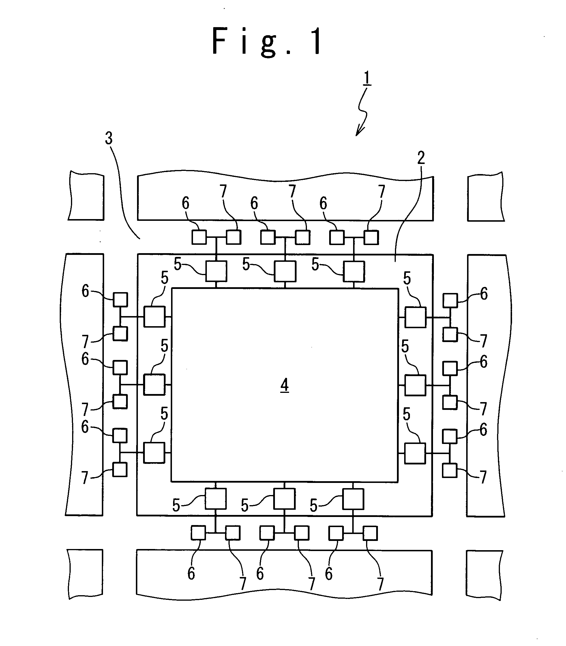
[0028] In one embodiment, as shown in FIG. 1, a semiconductor wafer 1 is subjected to a contact resistance test before a probing test of circuits integrated therein. The semiconductor wafer 1 is composed of a chip area 2 and scribe lanes 3. The chip area 2 is an area to be machined into a semiconductor chip through dicing. The chip area 2 is provided with an integrated circuit 4 and bonding pads 5. The bonding pads 5 are connected to the integrated circuit 4 to provide signal interface thereto. When the integrated circuit 4 is probe-tested, test probes are placed on the bonding pads 5. The scribe lanes 3 are disposed to provide areas where the semiconductor wa...


PUM


Abstract

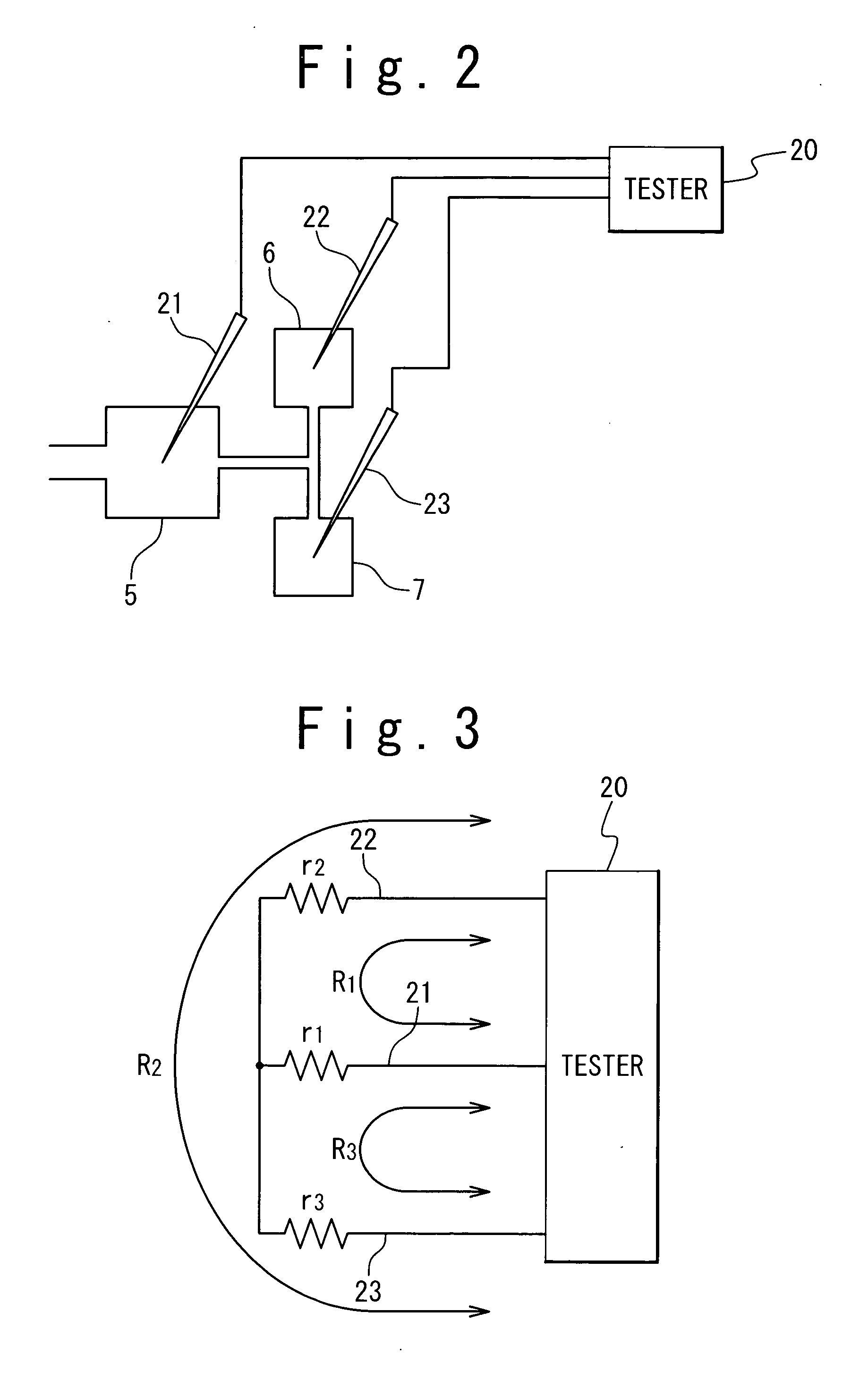
A contact resistance measurement method is composed of: placing a first probe onto a first pad connected to an integrated circuit; placing a second probe onto a second pad electrically connected to the first pad; placing a third probe onto a third pad electrically connected to the first pad; measuring a first resistance between the first and second probes; measuring a second resistance between the second and third probes; measuring a third resistance between the third and first probes. A contact resistance between the first probe and the first pad is calculated from the first to third resistances.

Description


Claims


Application Information

Patent Timeline
Owner NEC ELECTRONICS CORP
Learn More